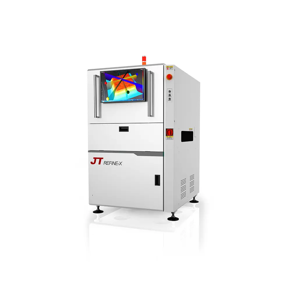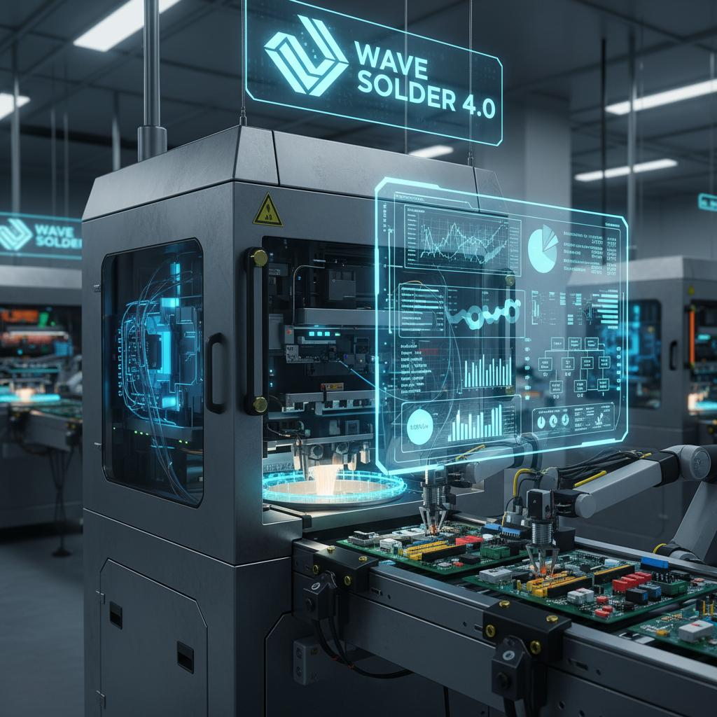

Automated Optical Inspection (AOI) has become an indispensable part of modern electronics manufacturing. As PCBs grow denser and component sizes shrink, manual visual inspection can no longer keep pace with the speed and precision that quality control demands. AOI vision inspection equipment addresses this challenge by combining high-resolution optics, intelligent lighting, and advanced image processing to detect solder joint and component defects automatically. This article explains the working principle of AOI equipment for solder joint and component inspection, and highlights how JT‘s AOI solutions put these principles into practice.

1. The Core Working Principle of AOI
AOI systems operate on a straightforward but powerful premise: a machine vision system captures images of the PCB, compares them against a set of reference criteria, and flags any deviations as potential defects. The workflow generally follows four stages:
-
Image acquisition – Cameras (typically high-resolution CCD or CMOS sensors) capture images of the board, often at multiple angles and magnifications.
-
Illumination control – Programmable lighting (such as multi-color LED arrays) illuminates the board from different directions to reveal solder shape, gloss, and component presence.
-
Image processing and analysis – Software algorithms extract features, compare them with programmed reference data, and classify results.
-
Defect reporting – Detected defects are marked, categorized, and reported for operator review or automatic disposition.
2. Solder Joint Inspection
Solder joint inspection is one of the most critical functions of AOI. Because solder joints are three-dimensional and reflective, AOI systems use a combination of techniques to evaluate them reliably:
-
Multi-angle imaging captures the joint from several viewpoints, allowing the system to assess fillet shape, wetting angle, and solder volume.
-
Color and intensity analysis distinguishes good joints (smooth, properly wetted) from defects such as insufficient solder, excess solder, cold joints, bridging, and voids.
-
3D measurement (in more advanced systems) provides height and volume data, enabling quantitative rather than purely visual judgment.
This approach allows AOI to detect common solder defects — including bridging, tombstoning, insufficient solder, solder balls, and cold solder joints — at production speed.
3. Component Inspection
Beyond solder joints, AOI equipment verifies that components are correctly placed and oriented. Key inspection items include:
-
Presence and absence of components
-
Position offset and rotation
-
Polarity and orientation (critical for diodes, capacitors, and ICs)
-
Component value and marking verification
-
Lead coplanarity and pin alignment for fine-pitch devices
By combining pattern recognition with reference data, AOI systems can reliably identify missing, misplaced, or wrongly oriented components.
4. Key Enabling Technologies
Several technologies work together to make AOI effective:
-
High depth of field optical systems ensure that components of varying heights remain in focus across the board.
-
Programmable multi-color lighting enhances contrast and separates solder from component surfaces.
-
Intelligent self-healing and robot integration allow modern systems to connect with welding robots, reducing maintenance time and cost.
-
Defect analysis and remote debugging support faster troubleshooting and continuous process improvement.
These capabilities are exactly where JT’s AOI equipment excels. According to JT, its AOI vision inspection equipment enables high-speed inspection with fully satisfied DIP production, and offers the advantage of performing post-soldering inspection without having to turn over the PCB. This not only saves handling time but also makes the process quicker and more efficient. JT’s equipment also features a high depth of field optical system and delivers significant financial benefits through reduced manpower requirements.
5. AOI in the Production Line
In practice, AOI equipment is typically deployed at several points in the SMT and DIP lines:
-
Post-print inspection (after solder paste printing)
-
Pre-reflow inspection (after component placement)
-
Post-reflow inspection (after soldering)
-
Post-DIP inspection (after wave or selective soldering)
Placing AOI at these checkpoints enables early defect detection, preventing defective boards from progressing downstream and reducing rework costs.
6. Why Choose JT’s AOI Vision Inspection Equipment
For manufacturers seeking reliable solder joint and component inspection, JT offers a wide range of AOI inspection and AOI equipment options to fulfill visual inspection and quality control needs. Key advantages include:
-
High-speed inspection with fully satisfied DIP production
-
Post-soldering inspection without PCB turnover, improving process speed and efficiency
-
High depth of field optical system for accurate imaging of varied component heights
-
Intelligent self-healing by connecting welding robots, reducing maintenance times and costs
-
Defect analysis and remote debugging features on selected devices
-
Reduced manpower requirements, delivering significant financial benefits
If you are looking for equipment that is smart, durable, efficient, and performs high-precision inspection, JT is the right place. You can visit JT’s website to browse the different AOI inspection equipment, check their features in detail, and get an AOI visual equipment quotation.
Conclusion
AOI vision inspection equipment works by combining high-resolution imaging, controlled illumination, and intelligent image analysis to verify solder joints and component placement automatically. By deploying AOI at key production checkpoints, manufacturers can detect defects early, improve yield, and reduce costs. With JT’s AOI inspection and AOI equipment — offering high-speed inspection, post-soldering inspection without PCB turnover, high depth of field optics, and intelligent self-healing — manufacturers can achieve efficient, cost-effective, and high-precision quality control. For more information, visit JT’s AOI vision inspection equipment page at https://www.jt-int.com/product-category/aoi-vision-inspection-equipment/.