
Solder paste printing is the first and most influential step in the SMT assembly process. Studies consistently show that the majority of soldering defects can be traced back to poor paste deposition — insufficient or excess paste, misalignment, smearing, or bridging. As components shrink and pin pitches tighten, these defects have moved beyond the range of human eyes. This is why Solder Paste Inspection (SPI) has become an essential part of modern SMT lines, and why 3D SPI equipment is now a standard investment for manufacturers committed to yield and reliability. This article explains the working principle of 3D SPI equipment and shows how JT‘s solder paste inspection machines apply these principles in production.
1. Why SPI Is Necessary
Over three decades of rapid SMT development, assembly methods have shifted from plug-in to SMD, component sizes have become smaller and smaller, and pin pitches have grown denser — exceeding what human vision can reliably recognize. Fine-pitch components such as QFP, and packages like PLCC and BGA with solder joints hidden beneath the body, create great difficulty for AOI inspection after mounting and after soldering. Many defects are only discovered after welding, making maintenance difficult and expensive. Combined with rising labor costs and industrial upgrading, introducing SPI machines into SMT production lines has become an inevitable trend.
2. The Core Working Principle of 3D SPI
A 3D SPI system measures the solder paste deposit in three dimensions rather than simply imaging it. The general workflow is:
-
Projection – A structured light pattern is projected onto the PCB surface and the paste deposits.
-
Image capture – Cameras record how the light pattern is deformed by the height of the paste.
-
3D reconstruction – Software reconstructs the surface profile of each deposit.
-
Measurement and comparison – Volume, area, height, and offset are calculated and compared against programmed tolerances.
-
Classification and reporting – Each deposit is judged pass or fail, and results are reported for process control.
Because it measures actual height and volume, 3D SPI can distinguish genuine defects from cosmetic variation — something 2D systems cannot do reliably.
3. White-Light Sine Stripe PMP Technology
JT’s 3D solder paste inspection is based on white-light sine stripe PMP (Phase Measuring Profilometry) technology. In this method, sinusoidal fringe patterns are projected onto the board, and the phase shift of the reflected fringes is analyzed to derive height information. The result is that inspection accuracy can reach 1 µm, and the system can auto-restore pad 3D data on the PCB surface, calculating the volume, area, height, and deviation of every solder paste deposit. This level of precision is what allows manufacturers to catch subtle deposition trends before they become defects.
4. 2D and 3D Fusion for Reliable Detection
Height measurement alone is not enough — the system must also recognize what it is looking at. JT SPI machines use four types of 2D light sources — R, G, B, and W — to make the image color more realistic, while the software algorithm applies 2D analysis to improve the recognition rate of bare copper, silk screen, bridging, and foreign objects. This fusion of 2D color information with 3D height data improves the detection rate and reduces misjudgment, which is critical for keeping false calls low on high-mix lines.
5. Programming and Usability
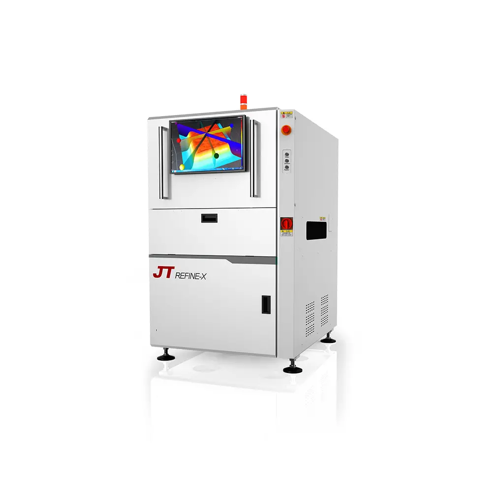
A capable SPI system must also be practical to program and operate. JT SPI machines use a graphic interaction interface with comprehensive functions that are easy to handle. In addition to programming with Gerber files, an image-oriented edit mode enables off-line programming and debugging, so line time is not consumed during program creation. A multi-touch function allows 3D image rotation and 2D image resizing, making it convenient to check and confirm solder paste conditions directly on screen.
6. SPC and Process Control
SPI is as much a process-control tool as an inspection tool. JT SPI machines include a comprehensive SPC function with many kinds of diagram generation and output. The SPC software records detailed data on volume, area, height, and offset of all solder paste on each PCB, enabling calculation of CPK and analysis and control of the front-end printing machine. In other words, SPI closes the loop: measurement data feeds back to the printer so that paste deposition stays within control limits.
7. Hardware Reliability
Measurement stability depends on mechanical stability. JT solder paste inspection machines feature image-accelerated calculations based on multi-GPU and an integrated cast iron frame structure whose high rigidity avoids outside vibration interference. This combination supports both fast computation and repeatable measurement in a busy production environment.
8. Why JT
JT has manufactured SPI machines since 2009, building strong R&D and production capability over more than a decade. JT’s SPI equipment delivers:
-
1 µm inspection accuracy based on white-light sine stripe PMP technology
-
Full 3D measurement of volume, area, height, and deviation for every deposit
-
Four-color 2D lighting (R, G, B, W) with 2D algorithms to improve recognition of bare copper, silk screen, bridging, and foreign objects
-
Off-line programming and debugging via Gerber files and image-oriented editing
-
Multi-touch 3D/2D visualization for convenient confirmation
-
Comprehensive SPC with CPK calculation to control the printing process
-
Multi-GPU acceleration and a rigid cast iron frame for stability
If you need a solder paste inspection machine, JT welcomes you to get in touch. You can browse JT’s SPI vision inspection equipment at https://www.jt-int.com/product-category/spi-vision-inspection-equipment/ to review the available models and their features in detail.
Conclusion
3D SPI works by projecting structured light onto the paste, reconstructing each deposit in three dimensions, and comparing measured volume, area, height, and offset against tolerances — with 2D color analysis added to confirm what is being measured. By catching printing defects before components are placed, SPI prevents expensive downstream rework and provides the process data needed for continuous improvement. With JT’s PMP-based 3D solder paste inspection machines — offering 1 µm accuracy, four-color 2D lighting, off-line programming, multi-touch visualization, and comprehensive SPC — manufacturers gain a practical, proven tool for controlling the front end of the SMT line.