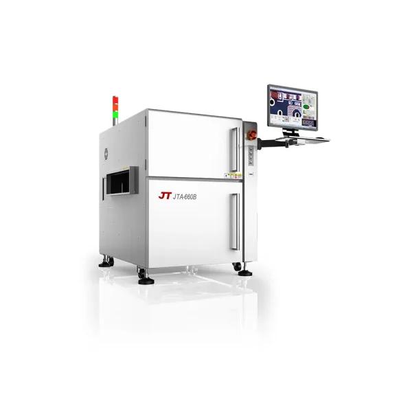
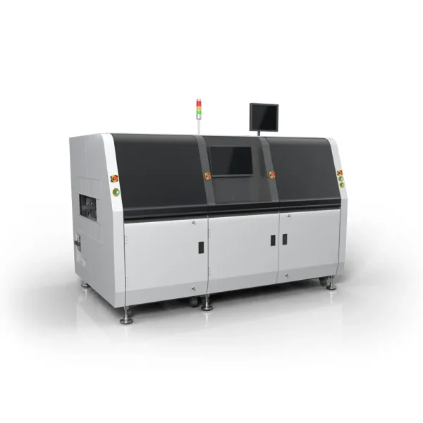
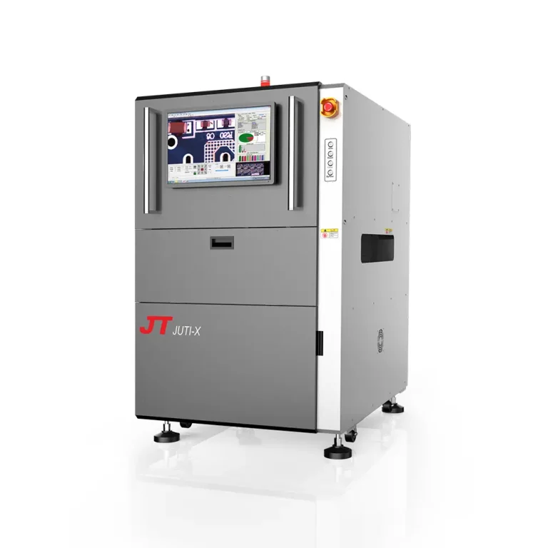
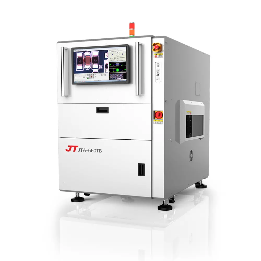
| Model | JTA-660B | |
| PCB Spec. | PCB Dimension | 50x50mm – 430x460mm |
| PCB Thickness | 0.5mm – 5mm(Standard) (5~20mm Customized) | |
| PCB Component height | Top 110mm Bottom 25mm | |
| PCB Warp | ±3mm | |
| Optical Parameter |
Resolution | 23μm(Standard) |
| Speed | 0.25 sec/FOV | |
| Camera Spec. | 5M High Speed Color Camera | |
| Optical Lens | Telecentric Optical Lens | |
| Light-Source | Multis pectral Super speed RGB+W Light Source | |
| Inspection Category | Component Inspection | ꢀMissing,ꢀRolling,Shifting,Polarity Error,Wrong Part,Damaged,Bended,PCB Abnormal,Residua,Glue Overflow |
| Solder Inspection | Excess Solder, Insufficient Solder,Bridging,Lifting,Solder Balls,Soldering Abnormal | |
| Special Inspection Items | Can Check Solder Paste and Epoxy Glue Process, Soldering Quality | |
| Hardware | X,Y Table Positioning Accuracy | ±0.01mm |
| X,Y Table Speed | 1000mm/s | |
| PCB Loading | Defined Mode: R->L / L->R | |
| PCB width adjustment | AUTO | |
| Main Frame Body | Whole Cast Iron Modeling | |
| Screwing-shaft | High precision ball screw | |
| Rail | High Level Rail | |
| Driver | AC Servo Motor | |
| OperatingSystem | Win 7 Professional | |
| Display | 22” LCD Monitor | |
| PowerSupply | AC 200-240V1Φ 50/60HZ | |
| Power | 1.8KW | |
| Pressure | 0.5MPa | |
| Dimension (W*D*H) | 1039x1483x1550mm | |
| Weight (KG) | 1000KG +/- 10KG | |
| Software | InspectionMethod | The Eigenvector Analysis & OCV Silkscreen Algorithm |
| InspectionAngleArea | 0-360°,Accuracy=1° | |
| MarkingFunction | One Board Marking & Multi-pieces Board Marking & Bad Marking, etc. | |
| ProgrammingMode | 1.CAD Coordinate Loading 2.Component Database Auto-index 3.Auto-programmingby Intelligent Software |
|
| RemoteControl | Network Monitoring: Offline Debugging, Online Monitoring & Manipulating, Remote Realized Examing | |
| DataRecording | Auto-generated Statistical Process Controlling Data (SPC) & Report | |
| Option | Barcode Scanner 1D/2Dꢀ(H/W) | Pin Support |
| Quality Tracing (Option) | Offline Programming System (PC) | |
| Three-point-verification System (Option) | 1D/2D Barcode Reading (S/W + License) | |
| The above contents are subject to change without further notice! | ||


MENU
PRODUCTS
CONTACT US
- Shenzhen JT Automation Equipment Co., Ltd.
- 0086-13570847602
- yxdsj01@jt-ele.com
- JT Industrial Park, Beiba Rd.,Hezhou Industrial Zone, Hangcheng, Baoan, Shenzhen
Copyright © Shenzhen JT Automation Equipment Co., Ltd.