Most of the amazing gadgets and devices that we use every day, including smartphones, tablets, computers, and even our TVs are built using a process called SMT. SMT, which stands for Surface Mount Technology, is one of the most important techniques used in electronics manufacturing today. It allows manufacturers to make smaller, faster, and more efficient electronic products. Let’s try to understand the SMT process flow and the different steps involved in it.
What is the SMT Process Flow?
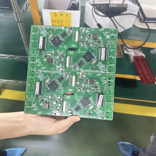
The SMT process flow is a series of steps that are used to place electronic components onto a printed circuit board (PCB). A PCB is like the skeleton of an electronic device that holds all the parts to make the device work. The SMT process flow includes several steps that need to be carefully followed so that the electronic components are placed in the right position and attached securely.

There are 5 steps involved in the SMT process flow:
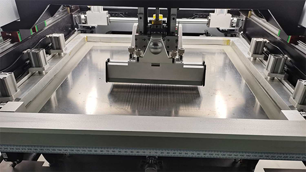
Solder Paste Printing
The first SMT process flow step is to apply solder paste to the surface of the PCB. This Solder paste is a mixture of tiny metal particles and flux, which is used to make the solder stick to the board. The solder paste is generally applied using a stencil that makes sure the paste only goes on the specific areas where components will be placed. This step makes sure that the components stick properly to the PCB.
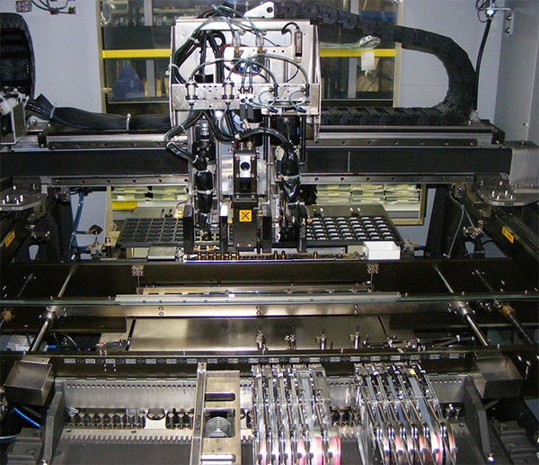
Component Placement
Once the solder paste is applied, the next step in the SMT process flow is to place the electronic components onto the board. This is done by using a special machine called a pick-and-place machine. This machine is quick, accurate, and used as an instrument to scoop up tiny electronic parts and drop them precisely where they should be on the PCB.
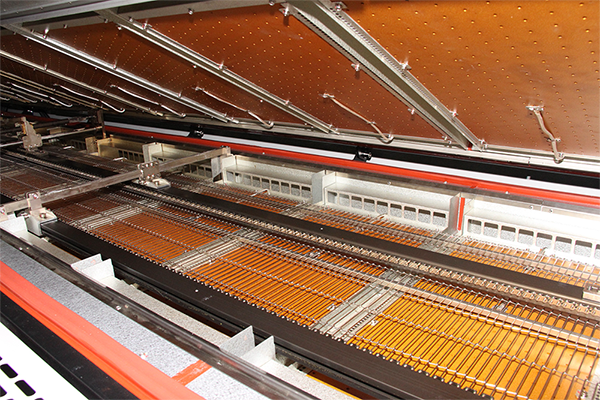
Reflow Soldering
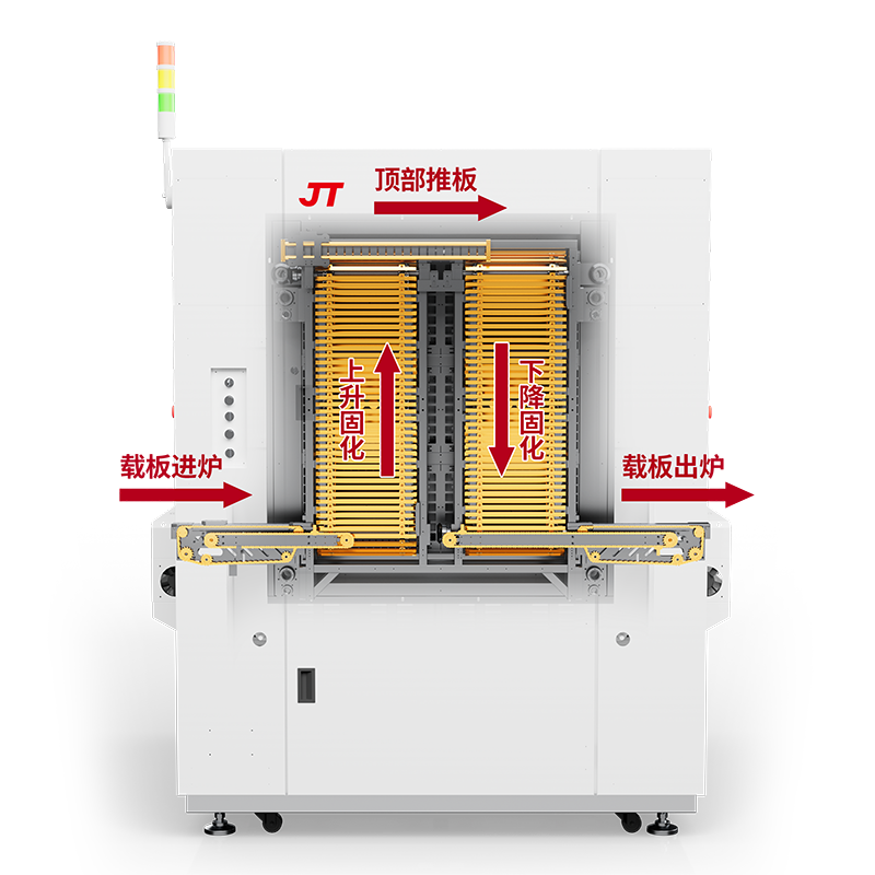
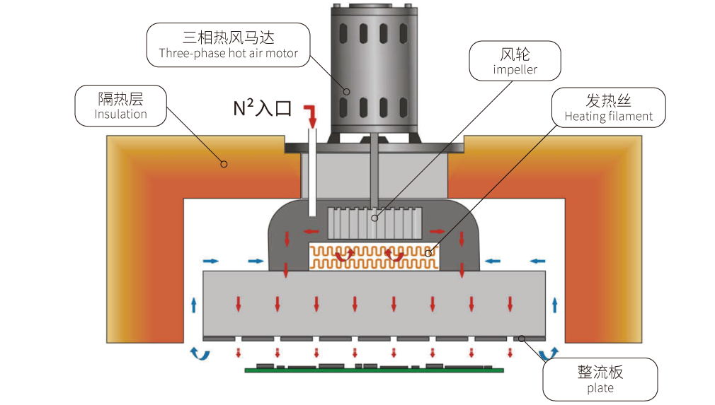
After the components are placed on the board, the next step is to heat the entire PCB in a special oven. This is called reflow soldering. During this step, the heat coordinates the process when the solder paste melts turning it down it forms stronger bands besides the components and the PCB. This is quintessential of the SMT process flow since it is the soldering of the parts that secures them so that they can’t drift or come apart.
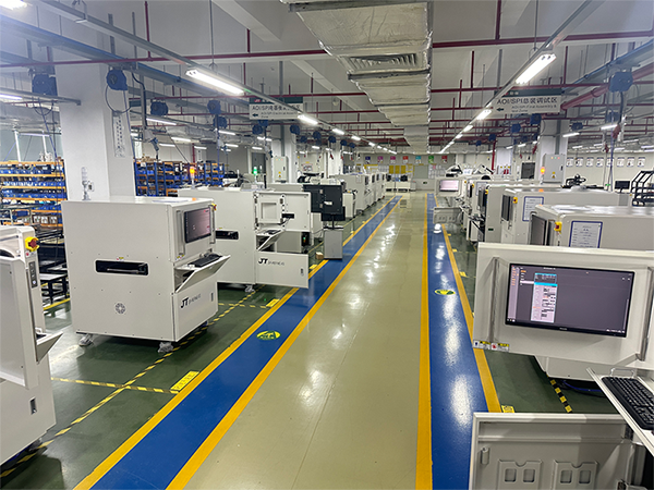
Inspection
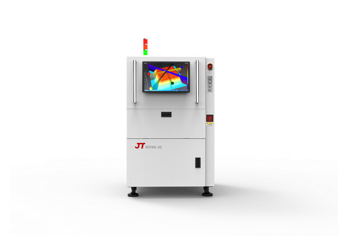
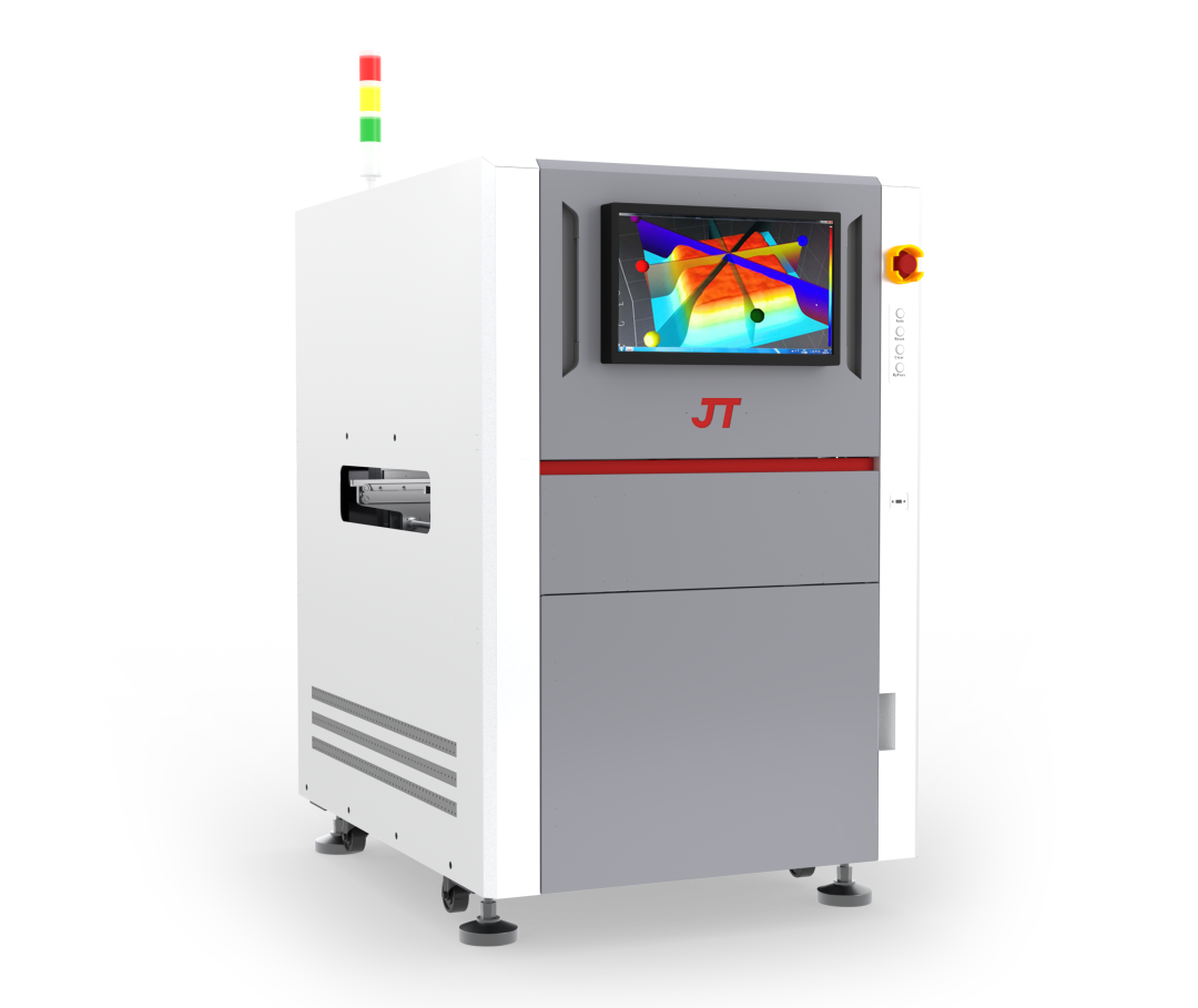
After the soldering is completed, the PCB assembly engages in an inspection process to verify correct placement and the absence of defects. This is done using Automated Optical Inspection (AOI) machines, which capture and process images of the board and determine if it is the same as a reference design. In the case of issues being notified, the problem can be resolved before the next step can be attempted.
Final Assembly
After the PCB has successfully passed all inspections and testing, the final assembly comes before. At this stage, the whole process involves locking the PCB structure in the casing or soldering the buttons, screens, or electrical connectors. The transfer tax is the step that lets us see this first base as a complete device that we can use.
Conclusion
The SMT process flow is a cornerstone of modern electronics manufacturing, enabling the creation of compact, reliable, and high-performance devices. With a commitment to precision and quality, JT delivers exceptional results at every stage of the process. By choosing JT, you’re partnering with a trusted manufacturer that ensures your electronic products meet the highest standards.