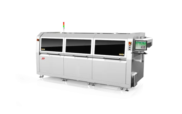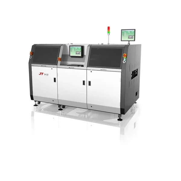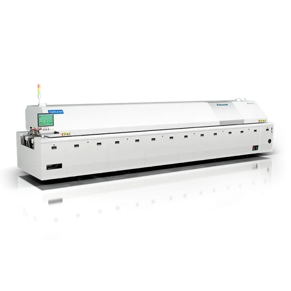

Wave soldering is a critical process in the assembly of printed circuit boards (PCBs), demanding precision and attention to detail to ensure quality and functionality. Understanding the step-by-step sequence is essential for achieving optimal results, particularly when comparing traditional soldering techniques like reflow soldering. The following is a detailed introduction by JT to the various stages of the wave soldering process:
1. Flux Application
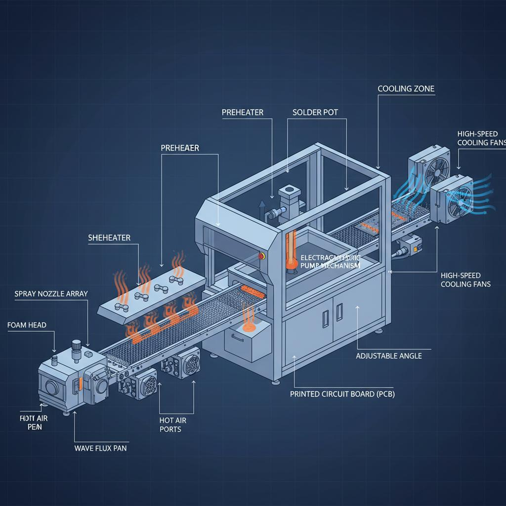
The first stage of the wave soldering process involves the application of flux to the PCB. Flux’s primary purpose is to clean the component leads and pads by removing oxides, thereby enhancing the wetting of solder. Critical parameters include flux type (rosin-based, water-soluble, etc.) and application method (spray or foam). The effect is immediate, ensuring surface readiness for soldering. For an in-depth understanding of flux application techniques, you may refer to our Wave Soldering Operation Guide.
2. Preheating
Preheating the PCB is crucial to prepare for solder wave contact. This step serves multiple purposes: it activates the flux, minimizes thermal shock to components, and reduces the risk of warping. Temperature control is critical, with typical preheat settings ranging from 100°C to 150°C. Immediate effects include increased component and flux stability. For more insights into temperature control mechanisms that are also pivotal in reflow techniques, see our article on the Critical Role of Chillers in Reflow Oven Temperature Control.
3. Solder Wave Contact
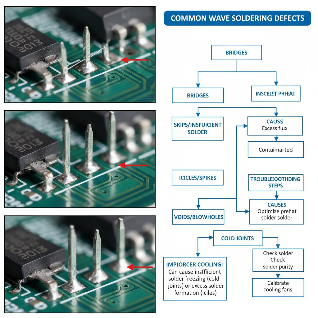
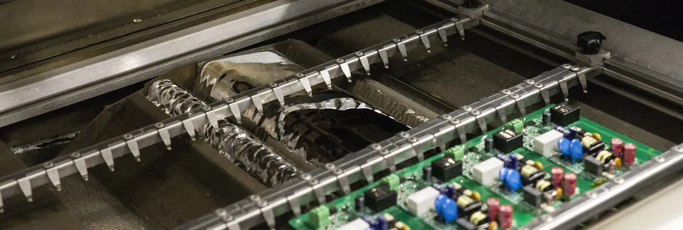
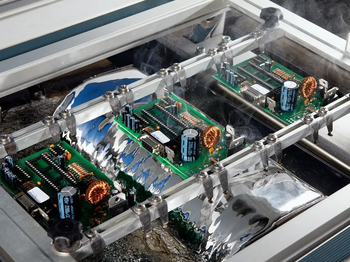
As the PCB moves across the solder wave, the molten solder forms fillets on the component leads and pads. The wave height, contact time, and conveyor speed are critical parameters, determining solder coverage and joint formation. The immediate effect is the creation of strong, conductive connections between components and the PCB.
Types of Solder and Flux in Wave Soldering: Selection and Application
Wave soldering is a critical process in PCB assembly, requiring precision in both the choice of solder and flux. Understanding these materials is essential for optimizing performance and complying with industry standards.
Solder Alloys in Wave Soldering
Solder alloys are a cornerstone of the wave soldering process, with options that include both leaded and lead-free. Each type offers specific benefits and challenges, impacting the choice based on application requirements and regulatory guidelines.
Leaded Solder Alloys (Sn-Pb)
Composition : Typically a mix of tin (Sn) and lead (Pb), commonly in a 63/37 ratio.
Advantages : Renowned for excellent wettability and thermal fatigue resistance.
Applications : Predominantly used in legacy electronics where RoHS compliance is not a constraint.
Considerations : Due to environmental regulations, its application is restricted, pushing industries towards alternatives.
Lead-Free Solder Alloys (SAC Alloys)
Composition : Commonly composed of tin (Sn), silver (Ag), and copper (Cu).
Advantages : Better thermal conductivity and mechanical strength, making them suitable for modern electronics.
Applications : Preferred in consumer electronics due to RoHS compliance. For insights on reflow techniques used with lead-free solders, refer to A Comprehensive Guide To The SMT Reflow Oven Process.
Considerations : Generally higher melting points compared to leaded alloys, requiring adjustments in process parameters.
Flux Types in Wave Soldering
Flux plays a pivotal role in ensuring effective soldering by cleaning and preventing oxidation. Understanding the types and their properties aids in selecting the right flux for specific tasks.
In-Depth Analysis
1. Rosin-Based Flux
Composition : Derived from natural resins mixed with activators.
Advantages : Provides excellent cleaning action and residue that can be accounted for in post-soldering operations.
Applications : Frequently used in high-reliability aerospace and military applications.
Optimizing Wave Soldering Parameters: Achieving Peak Performance
Wave soldering is a pivotal process in PCB assembly, and optimizing its parameters is essential for achieving superior performance and reliability. This section provides a detailed analysis of key parameters such as conveyor speed, preheat temperature profile, solder pot temperature, wave height, and wave contact time, offering practical guidance tailored to different PCB types and component characteristics.
Conveyor Speed
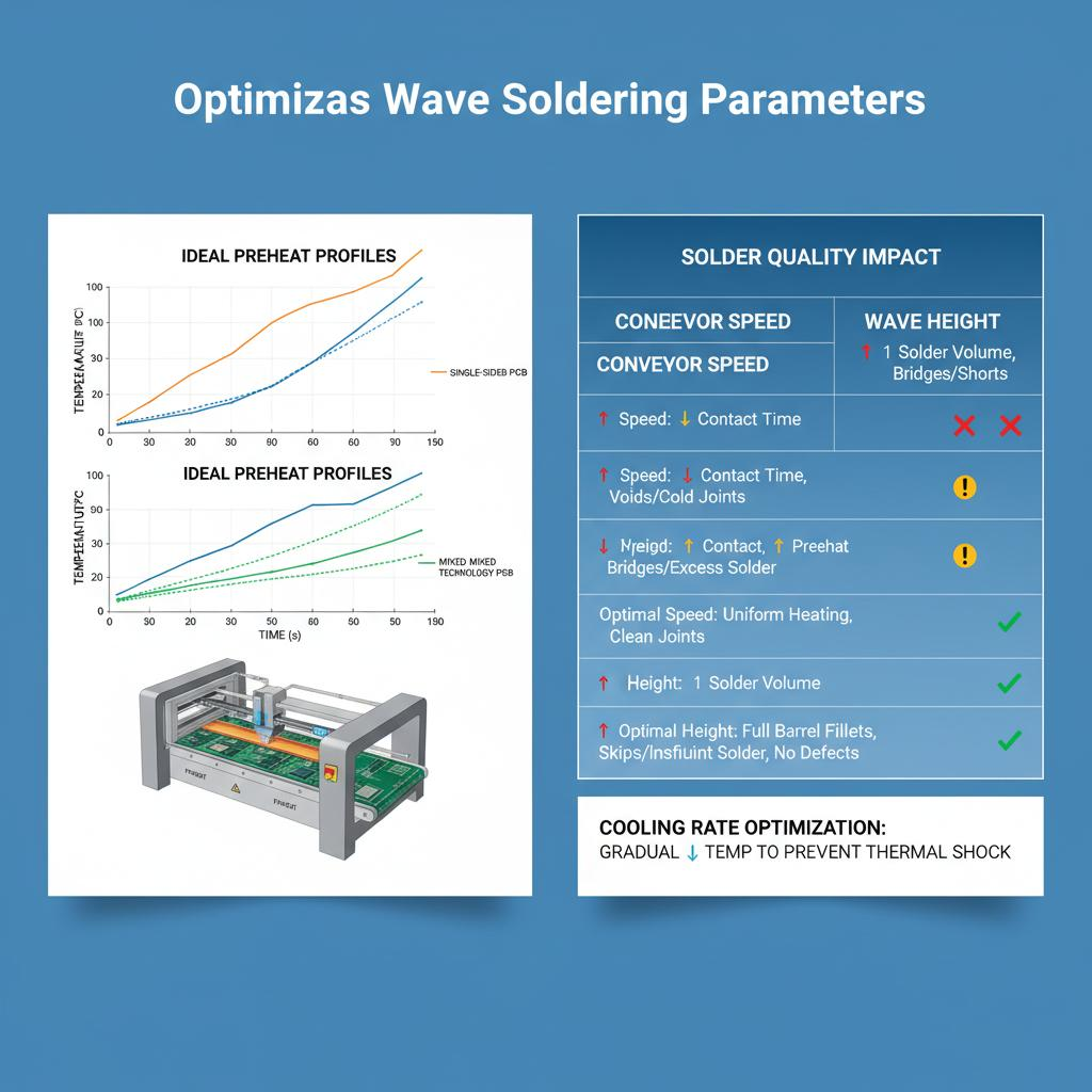
The conveyor speed is crucial as it influences the time components are exposed to the solder wave. For single-sided boards with larger components, a slower speed allows for better solder adhesion and minimizes the risk of solder bridges. Conversely, faster speeds may be implemented for double-sided boards or mixed technology assemblies where excess solder needs to be controlled to prevent clogging lead holes. For more detailed insights into conveyor systems and their optimization, you might find our article on Affordable PCB Conveyors helpful.
Preheat Temperature Profile
Preheating prepares the board and components for soldering by minimizing thermal shock. Ideal profiles differ based on PCB types and component sensitivity:
Single-Sided PCB: Utilize a gradual ramp-up temperature to ensure uniform heating.
Double-Sided or Mixed Technology: A steeper profile might be necessary to adequately heat components with higher thermal mass.
Adjusting the zone temperatures, particularly the peak temperature in the final zone, is vital to prevent component damage while ensuring the solder flows optimally. For those dealing with more complex soldering environments, consider the synergy between reflow ovens and chillers for precise temperature management, as discussed in our article on Reflow Ovens and Chillers.
Solder Pot Temperature
The solder pot temperature must be calibrated to the type of solder and flux used, but generally falls within the range of 240°-265°C for lead-free solder. It’s important to ensure it is consistently maintained to prevent oxidation and achieve uniform wetting.
Wave Height
Wave height directly affects solder application quality. Adjustments should be made based on board thickness and component clearance:
Thin Boards: Ensure lower wave height to avoid solder flooding.
Thicker Boards: Increase wave height to promote adequate penetration through plated-through holes.
Wave Contact Time
This parameter should be optimized to match the thermal mass of components. Components with higher thermal mass require longer contact times for effective soldering.