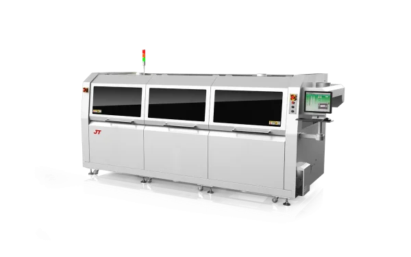

Wave soldering is a widely used method in electronics manufacturing for soldering components onto printed circuit boards (PCBs). While originally designed for through-hole components, it has become suitable over time for certain surface mount technology (SMT) components. Unlike reflow soldering, the primary soldering method for most SMT components, wave soldering is typically used for soldering specific SMT components located on the back of the PCB, such as chip resistors, capacitors, or connectors.
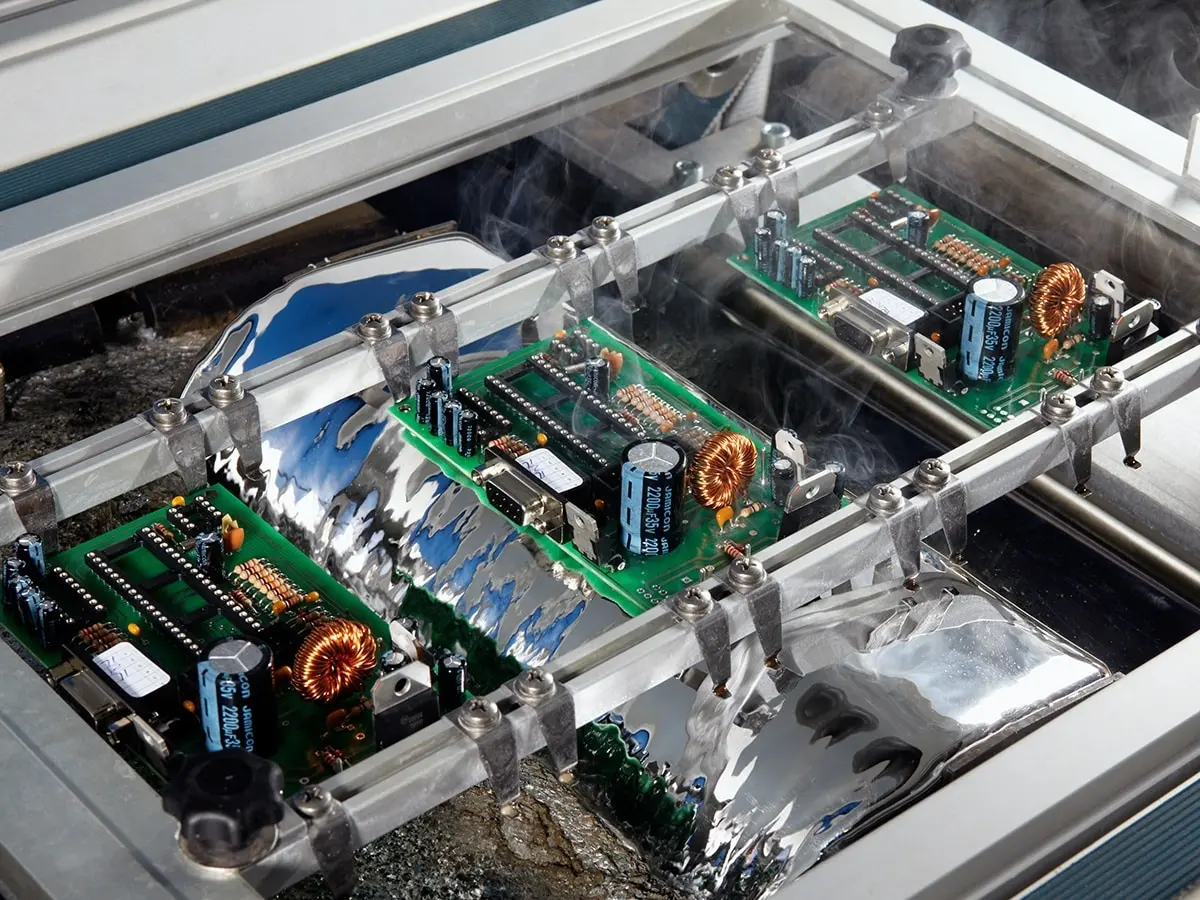
In the wave soldering process, a wave of molten solder passes over the PCB, attaching component leads or pads to the board. This process is fast and efficient, making it ideal for high-volume production. However, it requires careful preparation to ensure reliability, especially when handling SMT components.
Why is wave soldering used for SMT components?
While less common than reflow soldering, wave soldering is still suitable in certain situations. For example, it becomes a practical choice when the PCB contains both through-hole components and SMT components, or when specific SMT components such as connectors need to be soldered to the back of the board. In addition, wave soldering is more cost-effective for mass production because it can solder multiple components at once.
Understanding Wave Soldering Process
The wave soldering process involves several key steps to ensure components are securely and reliably attached to a printed circuit board (PCB). Below, we’ll explain each step in detail to help you understand how it works, especially when dealing with surface mount (SMT) components.
Step 1: Flux Application
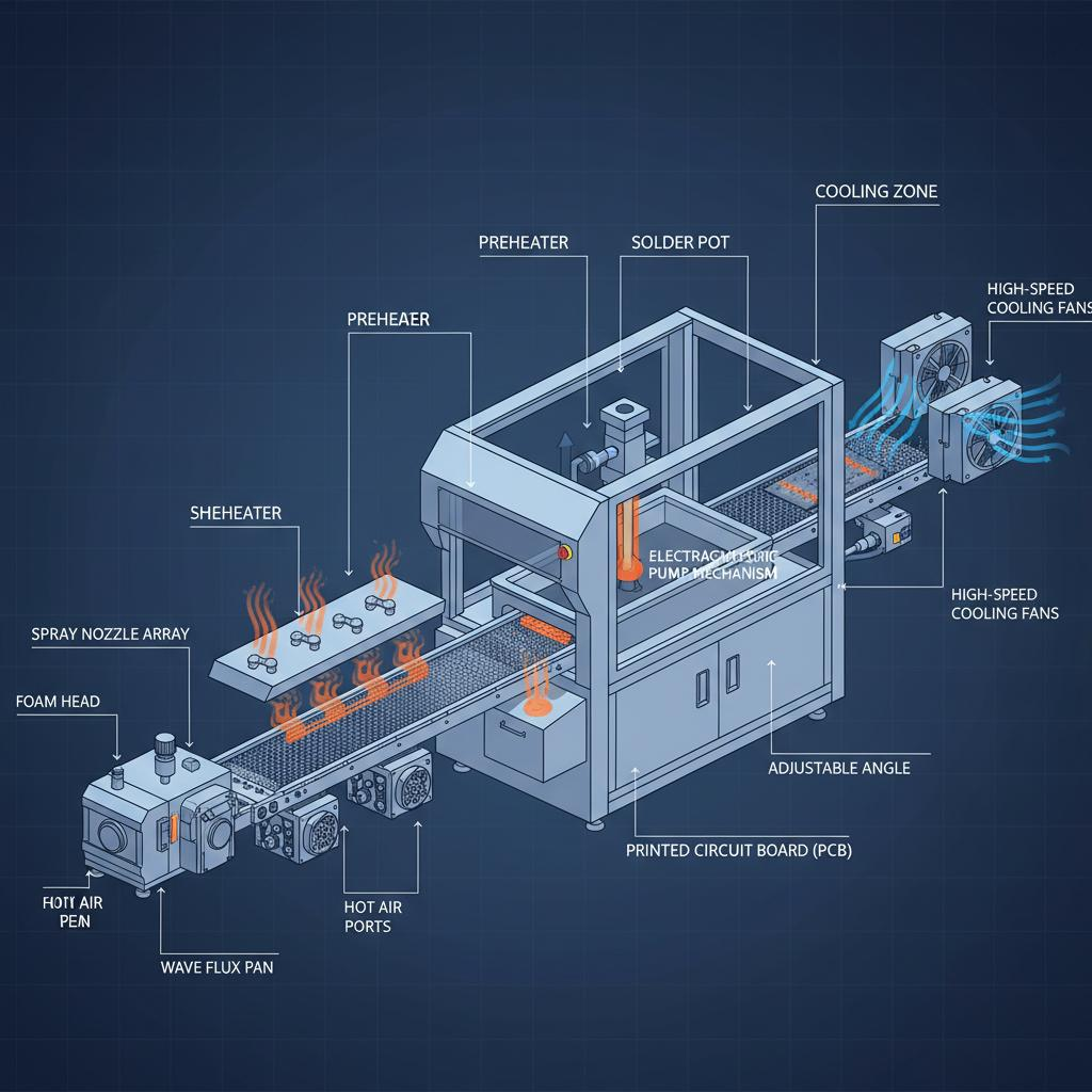
The first step in the wave soldering process is applying flux to the PCB. Flux is a chemical agent used to clean the metal surfaces of the circuit board and components, removing oxides and impurities to ensure better solder adhesion. For SMT components, flux is typically applied by spraying or foaming, ensuring even coverage of the back of the circuit board.
Step 2: Preheating the PCB
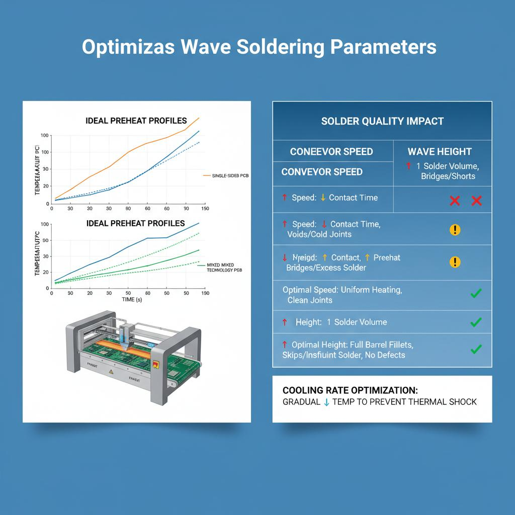
After applying flux, the PCB is preheated to between 100°C and 150°C, depending on the circuit board and components. Preheating prevents thermal shock when the circuit board comes into contact with the hot solder wave, avoiding damage to SMT components or poor solder joints. Furthermore, preheating activates the flux, preparing it for soldering.
Step 3: Wave Soldering Contacts
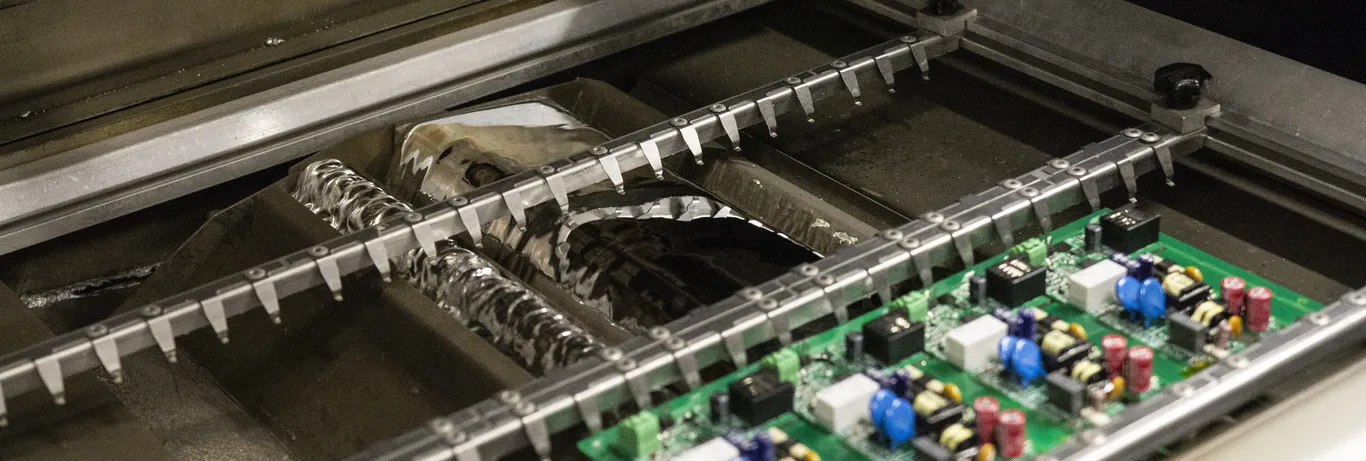
After preheating, the PCB board passes through a wave of molten solder. The temperature of the lead-free solder is typically maintained between 250°C and 260°C. This wave of solder is generated by a pump within the soldering machine, which pushes the molten solder upwards through nozzles. As the PCB board passes through, the solder adheres to the exposed metal pads and component leads, forming a strong electrical connection.
For SMT components, due to the lack of mechanical stability of through-hole leads during wave soldering, this step usually requires the use of adhesive dots to hold the components to the back of the board.
Step 4: Cooling
After passing through the solder wave, the PCB board enters the cooling zone. The cooling zone solidifies the solder, thus firmly securing the components in place. Controlled cooling is crucial to prevent excessive stress on the board or components, which could lead to cracks or loose solder joints.
Step 5: Cleaning
Finally, the PCB is cleaned to remove residual flux or contaminants. This step is especially important in wave soldering because excessive flux can lead to corrosion or electrical problems over time. Cleaning is typically done using solvents or water-based solutions, depending on the type of flux used.