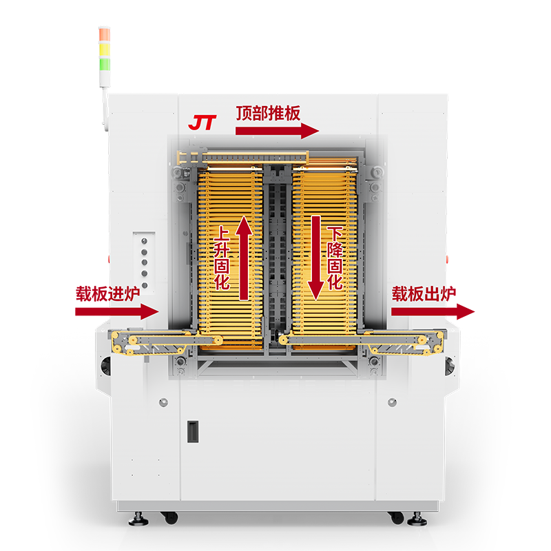
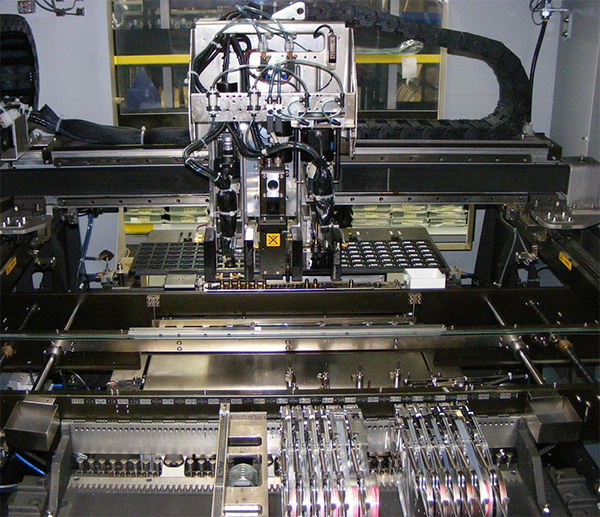
How is 3D SPI Involve in SMT Process?
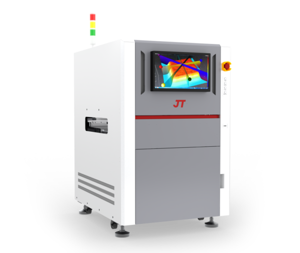
3D SPI stands for three-dimensional solder paste inspection. It’s a process used in Surface Mount Technology (SMT) to check the volume, height, and area of solder paste deposits on a PCB. These parameters are crucial because they affect how well components attach to the board during the reflow soldering process.
Unlike traditional two-dimensional inspections, 3D SPI provides a more comprehensive analysis. It uses advanced imaging to create a detailed map of the solder paste, highlighting even minor deviations. This level of precision helps manufacturers identify and correct issues early, saving time and reducing waste.
Difference Between AOI and SPI
Although AOI (Automated Optical Inspection) and SPI (Solder Paste Inspection) both focus on quality control in electronics manufacturing, they serve distinct purposes. Understanding their differences is key to optimizing the production process.
- Function: SPI is dedicated to inspecting solder paste deposits before components are placed on the PCB. It ensures that the volume, height, and alignment of solder paste meet the necessary standards. AOI, on the other hand, checks for defects after components are mounted. It inspects solder joints, component positioning, and overall assembly.
- Technology: SPI uses 3D imaging techniques to measure solder paste properties in detail. AOI primarily relies on cameras and 2D or 3D imaging to detect visual defects in the final assembly.
- Timing: SPI occurs early in the SMT process, allowing manufacturers to address solder paste issues before they escalate. AOI happens later, providing a final quality check before the product moves to the next stage.
Applications of 3D SPI in SMT
3D SPI has become an integral part of modern SMT (Surface Mount Technology) processes. Its applications span various stages of electronics manufacturing and contribute significantly to product reliability.
- Quality Assurance: SPI helps maintain consistent solder paste application, a critical factor in avoiding weak solder joints or component misalignments.
- Process Optimization: By identifying issues like insufficient paste or misaligned deposits, SPI enables manufacturers to fine-tune their processes. This reduces waste and improves efficiency.
- High-Volume Production: In large-scale manufacturing, SPI ensures every board meets the same high standards, minimizing variability between batches.
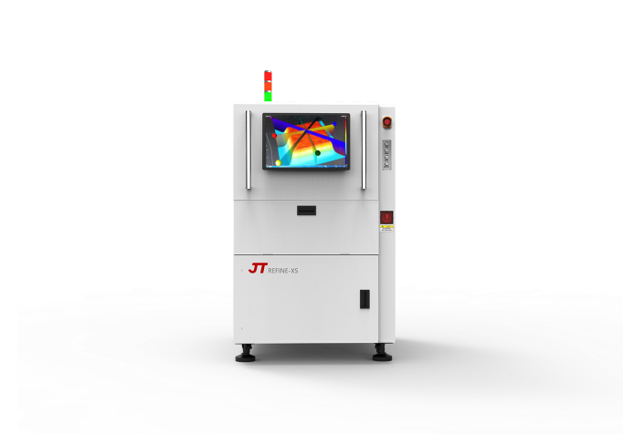
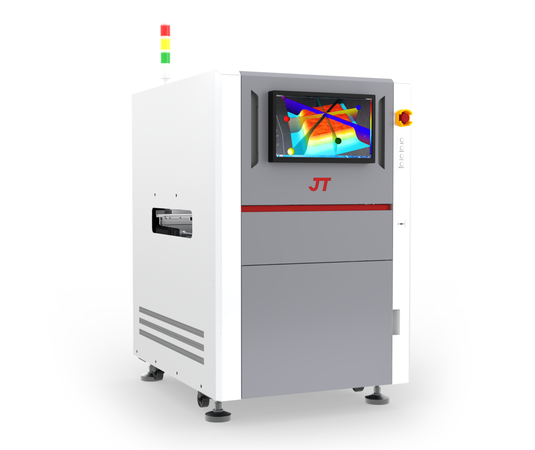
Advantages of 3D SPI Technology
3D SPI technology offers numerous benefits that enhance the efficiency and reliability of electronics manufacturing. Here’s why it’s a game-changer:
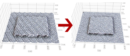
- Unparalleled Precision: By capturing 3D data, SPI provides detailed measurements of solder paste deposits, highlighting even minor deviations.
- Early Defect Detection: Identifying issues early in the process reduces the likelihood of costly rework or product failure later.
- Speed and Efficiency: Modern SPI systems operate at high speeds, making them suitable for large-scale production environments.
- Enhanced Process Control: SPI systems generate valuable data that manufacturers can use to optimize their processes and improve long-term performance.
- Reduced Costs: By minimizing defects and rework, SPI helps manufacturers save on materials, labor, and time.
Challenges in Implementing 3D SPI
Implementing 3D SPI technology comes with challenges that require careful consideration. A major obstacle is the high initial cost of advanced SPI systems, which can deter smaller manufacturers. However, the long-term benefits, including improved efficiency and reduced defects, often outweigh the upfront investment.
Training staff to maintain and operate these systems effectively is also crucial for consistent performance. Additionally, integrating 3D SPI into existing production lines may require workflow adjustments and compatibility checks, but careful planning can ease the transition and maximize efficiency.