
Tombstone Effect
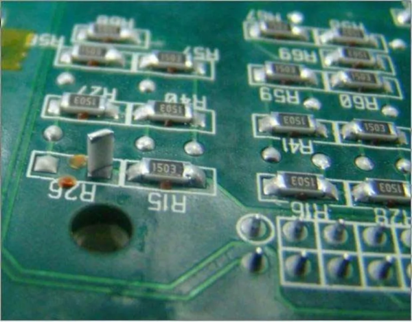
The tombstone effect, also known as the Manhattan effect or bridging effect, is a common reflow soldering defect. It occurs when one end of a surface-mount component (usually a chip resistor or capacitor) tilts up and stands vertically on the PCB. This can lead to open circuits and potentially cause electronic component failure.
Factors contributing to the tombstone effect include:
Uneven Heating: If one side of a component reaches the solder melting point faster than the other, the surface tension of the molten solder pulls the component towards a vertical position. Ensuring a uniform reflow oven temperature profile that matches the solder paste and component specifications helps mitigate this problem.
Uneven Wetting: Different wetting rates at the ends of a component can also cause tombstoneing. Factors affecting wetting rate include component and pad geometry, solder paste composition, and PCB surface finish. To address this, stencil design must be optimized, appropriate solder paste selected, and a consistent PCB surface finish ensured.
Component and Pad Misalignment: Misalignment of components or pads can lead to uneven solder distribution, increasing the probability of the tombstone effect. Precise component placement and proper pad design during the surface mount process are crucial for reducing the occurrence of such defects.
Pad and Component Size: Using components with larger volumes or wider terminals helps improve component stability during reflow soldering, thereby reducing the risk of tombstoning. Furthermore, ensuring pad size compatibility with the selected components helps maintain a balanced solder distribution.
To minimize the occurrence of tombstoning, it is essential to understand and control the factors that lead to this defect. Implementing robust quality assurance procedures, monitoring the reflow soldering process, and improving process parameters based on feedback can significantly reduce the incidence of tombstoning and improve the reliability of the final electronic assembly.
Voids
Voids refer to air pockets or gas-filled gaps within the solder joint during reflow soldering. They adversely affect the electrical and thermal properties of the solder joint, leading to reduced reliability or even failure of the electronic assembly. Voids can occur in various solder joints, but are most common in Ball Grid Array (BGA) and Quad Flat No-Leader (QFN) packages.
Causes of Voids: Several factors can lead to void formation:
Gas Escape: Gases generated during reflow soldering, whether from the solder paste or the components themselves, can become trapped within the solder joints. This occurs if poor ventilation or excessively viscous solder paste prevents gas escape.
Oxidation: Oxide layers on component leads, pads, or solder balls can hinder adequate wetting of the solder paste, creating voids within the solder joints. Proper storage and handling of solder paste and components helps minimize oxidation-induced voids.
Solder Paste Handling and Storage: Improper handling or storage of solder paste, such as exposure to humidity or temperature fluctuations, can alter its viscosity and consistency, resulting in voids. Ensuring solder paste is stored according to the manufacturer’s instructions helps reduce void formation.
Solutions to Reduce Voids: Implementing various process improvements can help reduce void formation:
Optimizing Reflow Soldering Temperature Profile: Adjusting the reflow oven temperature profile to allow for a gradual increase in temperature and maintaining it above the solder melting point for a sufficient time allows for more efficient gas escape, reducing the likelihood of void formation. Solder Paste Selection: Choosing a solder paste with low-voidity properties, such as a low-voidity formula or one with appropriate flux chemistry, can help minimize voids.
Stencil Design and Printing: Ensuring correct stencil design, such as aperture size and shape, and maintaining consistency in solder paste printing, allows for more uniform solder deposition and reduces voids.
Component and PCB Preparation: Ensuring components and PCBs are free of contaminants and oxide layers improves wettability and reduces void formation. This can be achieved through proper handling, storage, and cleaning procedures.
By understanding the factors that contribute to void formation and implementing appropriate process controls and improvements, manufacturers can effectively reduce voids in solder joints, resulting in more reliable and robust electronic components.
Solder Balls
Solder balls are small, unintended solder balls that form during reflow soldering. These solder balls can cause short circuits, reduced solder joint strength, and decreased reliability of electronic components. Understanding the causes of solder balls and potential solutions is crucial for achieving high-quality solder joints and reliable electronic products.
Causes of Solder Ball Formation: Solder ball problems are common in DIY soldering techniques, violating IPC standards. Other factors can also lead to solder ball formation:
Solder Paste Flux Activity: The flux in solder paste plays a crucial role in reducing oxides on the solder surface. However, if the flux activity is too high or the viscosity is insufficient, it can cause molten solder to separate and form individual spherical particles.
Solder Particle Oxidation: Oxidation on the surface of solder particles hinders coalescence during reflow soldering, leading to solder ball formation. Proper storage and handling of solder paste helps minimize oxidation.
Solder Paste Printing Accuracy: Incorrect or inconsistent solder paste application can cause solder balls to form during reflow soldering. Ensuring accurate and well-designed stencil printing helps reduce solder ball formation.
Reflow Profiling: An inappropriate reflow temperature profile can cause the solder paste to melt too quickly or fail to fully fuse, resulting in solder balls.
Solutions to Solder Ball Problems: Implementing process improvements can help reduce solder ball formation:
Solder Paste Selection: Choosing a solder paste with suitable flux activity and viscosity helps prevent solder ball formation. Manufacturers should consider the specific requirements of their application and consult solder paste suppliers for advice.
Optimizing Reflow Profiling: Adjusting the reflow oven temperature profile to ensure a gradual temperature increase and maintaining sufficient time above the solder melting point promotes adequate solder coalescence, reducing solder ball formation.
Stencil Design and Printing: Ensuring correct stencil design, such as opening size and shape, and maintaining consistent solder paste printing results in more uniform solder deposition and reduced solder ball formation.
Component and PCB Surface Finishing: Ensuring that component and PCB surfaces are free of contaminants and oxide layers improves wettability and solder fusion, reducing the likelihood of solder ball formation. Proper handling, storage, and cleaning procedures are crucial for maintaining surface quality.
By understanding the factors that contribute to solder ball formation and implementing appropriate process controls and improvements, manufacturers can effectively reduce solder ball formation and improve the reliability of electronic components.