Optimizing reflow soldering for high-quality PCB assembly requires controlling solder paste and stencil design, stabilizing oven temperature profiles and conveyor speed, ensuring precise component placement, and using AOI and X-ray inspection to detect and eliminate defects after reflow.
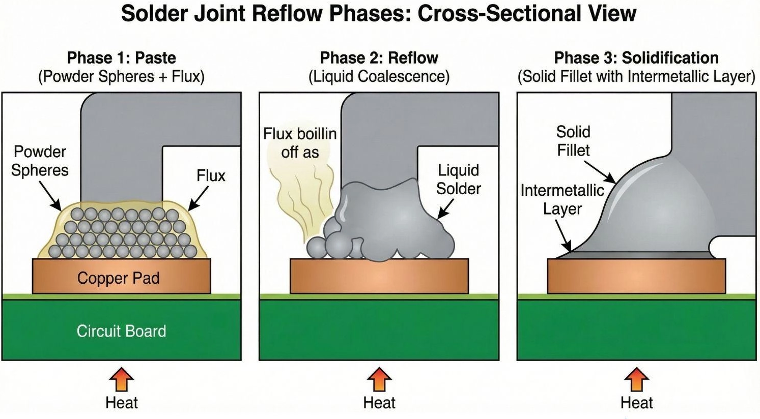
Optimizing solder paste selection and stencil design
Reflow soldering quality improves when the correct solder paste and well-designed stencil apertures are used to ensure accurate paste volume and uniform deposition.
In SMT reflow soldering optimization, solder paste selection is critical. The particle size of solder paste in PCB assembly must match the component pitch—smaller particles are used for fine-pitch ICs to ensure smooth printing and better melting behavior.
Flux composition also plays an important role. A well-balanced flux helps remove oxidation and improves solder wetting during the reflow stage, reducing defects like weak joints or non-wetting.
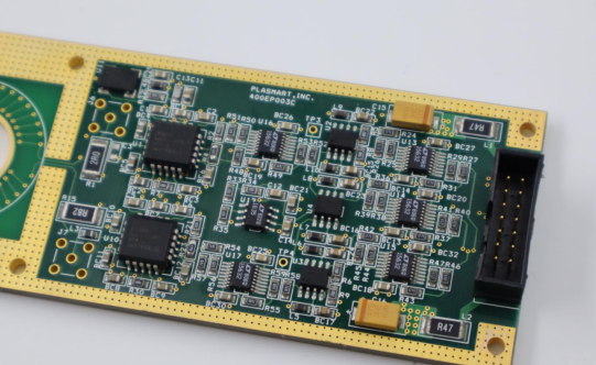
Stencil design directly controls how much solder paste is applied. Aperture design accuracy in stencil printing ensures each pad receives the correct paste volume. For example, in HDI PCB manufacturing, reducing aperture size slightly helps prevent solder bridging between closely spaced pads.
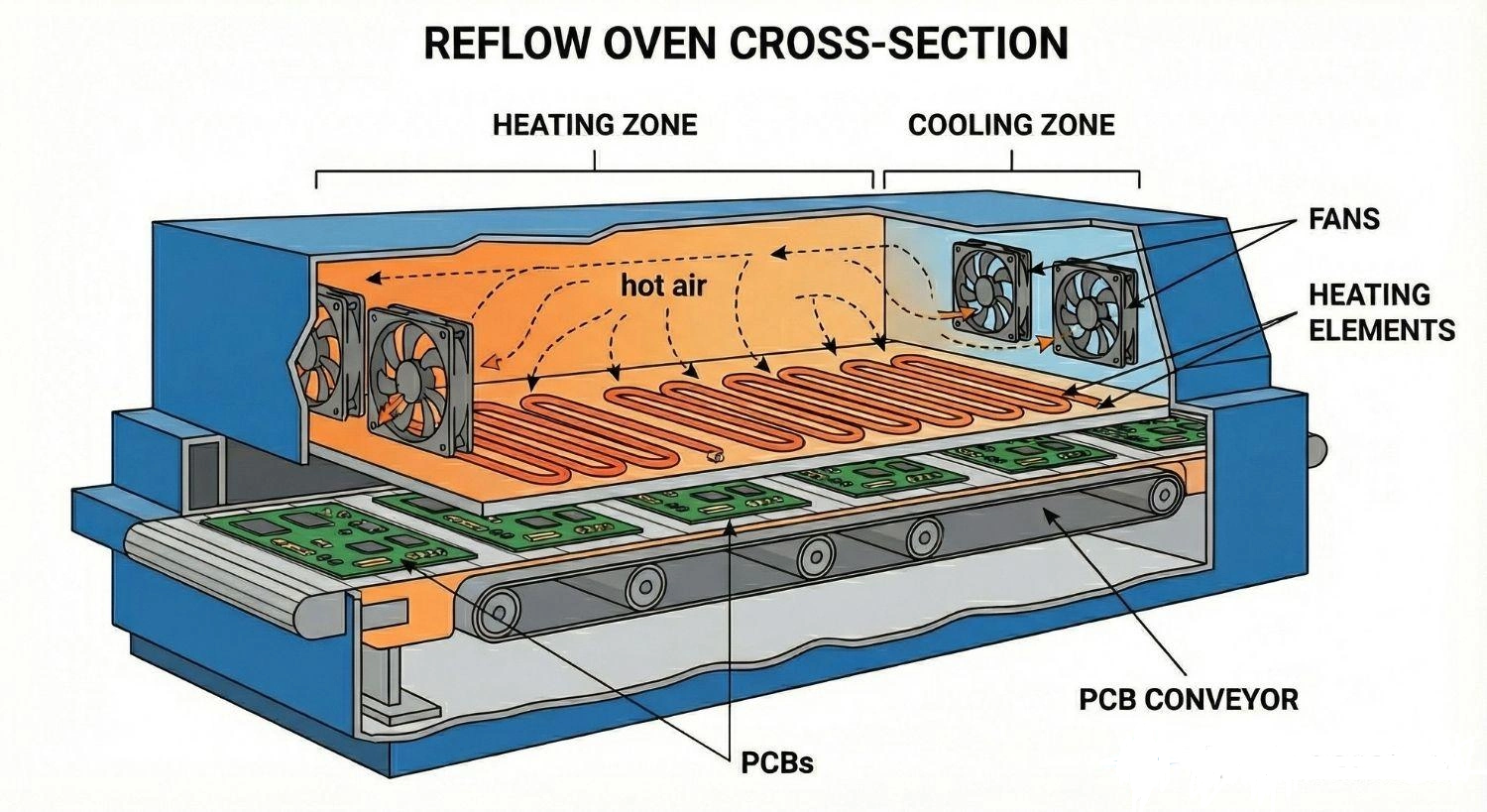
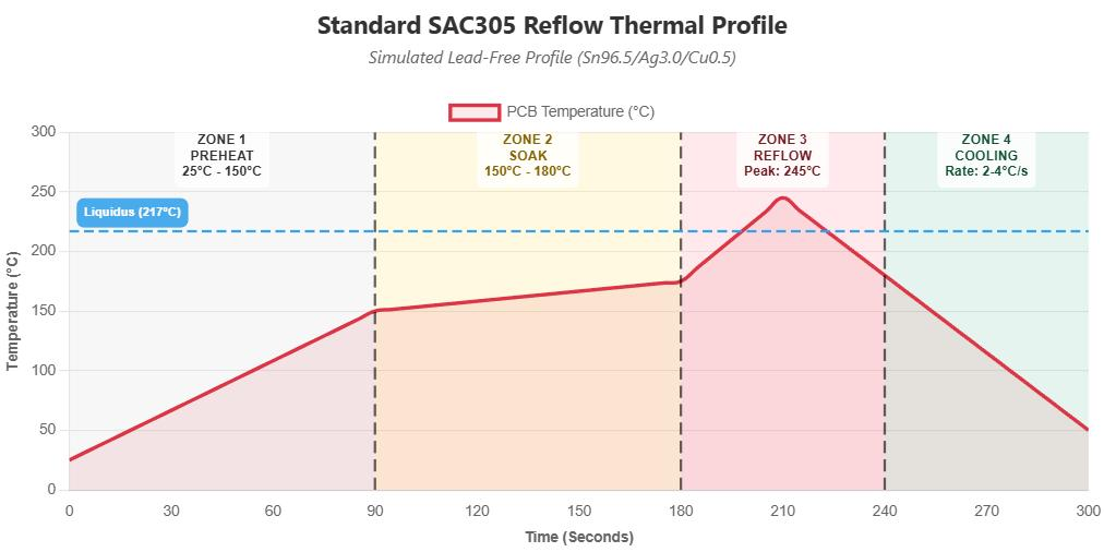
Adjusting conveyor speed and oven zones for process stability
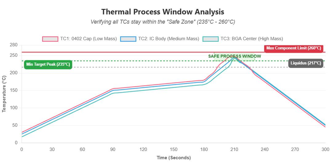
Stable reflow soldering requires properly balanced conveyor speed and oven temperature zones to ensure consistent heating across all PCBs.
In a reflow oven process control system, conveyor speed determines how long a PCB stays in each heating zone. If the speed is too fast, the board may not reach proper solder melting temperature; if too slow, components may overheat.
Each oven zone (preheat, soak, reflow, cooling) must be carefully tuned to maintain a stable SMT thermal profile consistency. This ensures every PCB receives the same heat exposure.
For example, in high-volume consumer electronics production, even a small change in conveyor speed can affect thousands of boards per hour, making process stability essential for yield control.
Component placement accuracy and its impact on yield
High placement accuracy ensures components align correctly with solder paste, directly improving yield and reducing defects after reflow.
In pick-and-place systems for PCB assembly, placement accuracy refers to how precisely components are positioned on solder paste pads. Modern SMT machines use vision alignment systems to achieve micron-level precision.
If placement is off, defects such as solder bridging, open joints, or tombstoning can occur after reflow. This is why component placement tolerance in SMT manufacturing is tightly controlled.
For example, in automotive ECUs, even slight misalignment of ICs can lead to long-term reliability failures under vibration and thermal cycling. High-precision placement significantly reduces rework and improves production yield.
Using inspection systems after reflow (AOI and X-ray)
Post-reflow inspection systems like AOI and X-ray are used to detect solder defects that are not visible or difficult to identify with the naked eye.
In automated optical inspection (AOI) for PCB assembly, high-resolution cameras scan the PCB surface to detect visible defects such as solder bridging, missing components, or misalignment.
For hidden joints like BGA (Ball Grid Array) components, X-ray inspection in SMT manufacturing is required. It allows manufacturers to see inside solder joints and detect voids, cracks, or incomplete bonding.
For example, in server motherboard production, X-ray inspection is critical because BGAs cannot be visually inspected after reflow, yet they carry high-speed signal integrity requirements.
Together, AOI and X-ray systems form a complete quality control loop that ensures high-reliability reflow soldering results in PCB production.