
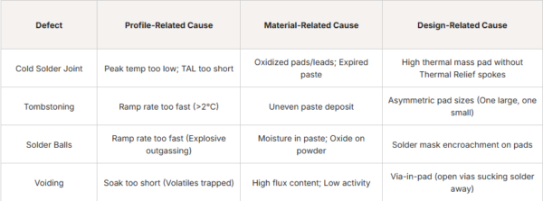
Even with perfect equipment, physics can be unforgiving. Identifying the root cause is key to prevention.
Tombstoning (The Manhattan Effect)
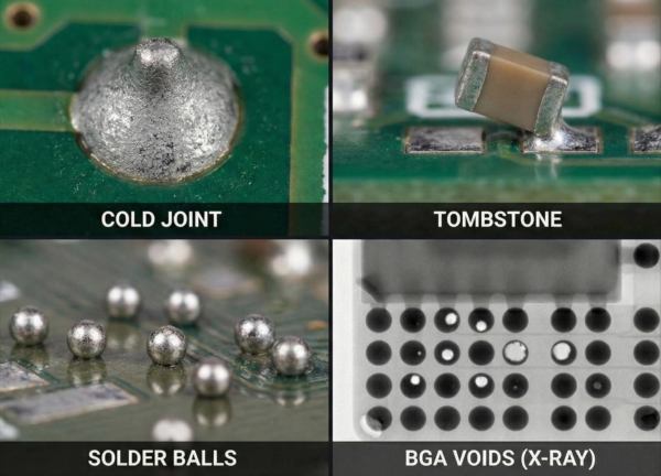
Symptom: A small passive component (0402/0603) stands vertically on one end, looking like a tombstone.
Root Cause: Torque imbalance. The solder on one pad melted and wetted before the other. The surface tension pulled the component upright.
Fix:
● Design: Ensure pads have symmetric thermal connections. Don’t connect one pad to a massive ground plane without thermal relief spokes.
● Process: Slow down the ramp rate into reflow to ensure both pads reach the liquidus simultaneously.
Solder Balling
Symptom: Tiny spheres of solder scattered around the joint or on the soldermask.
Root Cause:
● Explosive Outgassing: Ramp rate too fast (>3°C/s) trapped solvents.
● Oxidation: Solder powder oxidized (paste mishandling).
Fix: Check the preheat slope and ensure the paste was stored/thawed correctly.
Voiding (Gas Pockets)
Symptom: Empty cavities inside the solder joint, visible only via X-ray. Critical for QFN thermal pads.
Root Cause: Flux volatiles trapped during the liquid phase.
Fix:
● Increase the soak time to allow volatiles to escape before reflow.
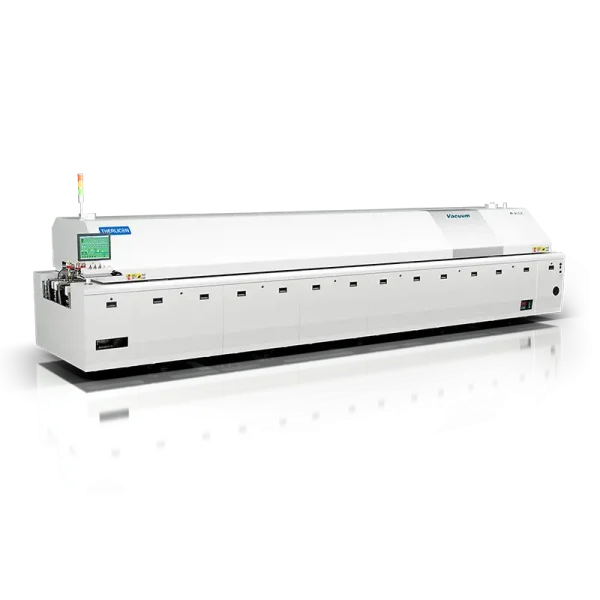
● Use a “Vacuum Reflow” process for critical power electronics (removes voids by pressure differential).
Head-in-Pillow (HiP)
Symptom: A BGA ball rests on the pad but hasn’t coalesced with the paste. It looks like a head resting on a pillow.
Root Cause:
1. Warpage: The BGA warped (smiled/frowned) during heating, lifting the ball off the paste.
2. Flux Exhaustion: The flux dried out before the ball touched the paste.
Fix: Verify moisture sensitivity handling (MSL) and optimize the soak profile to be shorter/cooler.
Quality Control and Inspection in Reflow Soldering
You cannot improve what you cannot measure. Post-reflow inspection is the gatekeeper of quality.
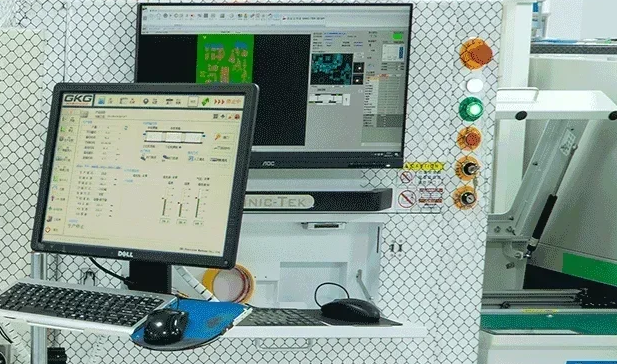
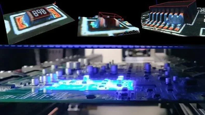
1. AOI (Automated Optical Inspection): Cameras scan the board using different angles of light. They check for component presence, polarity, skew, and visible solder fillets.
2. AXI (Automated X-Ray Inspection): Mandatory for BGAs, QFNs, and LGAs. The X-ray technology used here will go through the protective layers and show the percentage of voiding and bridging, as well as the presence of HiP defects, if any, underneath.
3. Electrical Testing (ICT/Flying Probe): Checks if the physical connection conducts electricity.
DFM Best Practices for Reflow Soldering
Certain golden rules constitute success criteria for a reflow process:
1. Solder Paste Handling: Paste is perishable. Keep it refrigerated (2-10℃).
Crucial: Allow it to thaw naturally for 4 hours before opening the jar. Opening a cold jar induces condensation, adding water to the paste → immediate Solder Balling.
2. Stencil Design: For fine-pitch components, the stencil aperture should be slightly smaller than the pad (e.g., 10% reduction) to prevent bridging.
3. Thermal Reliefs: Always use thermal spokes when connecting pads to ground planes. This is the #1 way to prevent cold joints and tombstoning.
Conclusion
Reflow soldering is a triumph of material science and process engineering. It allows us to manufacture reliable electronics at a scale and density previously impossible. However, it requires respect for the “Process Window.” From the thixotropic properties of the paste to the grain structure formed during cooling, every variable matters.
The point that, for designers, is pretty obvious is that DFM starts layout-wise. Thus, besides the schematic itself, one must take into consideration symmetric pads, proper thermal reliefs, and component spacing as well.