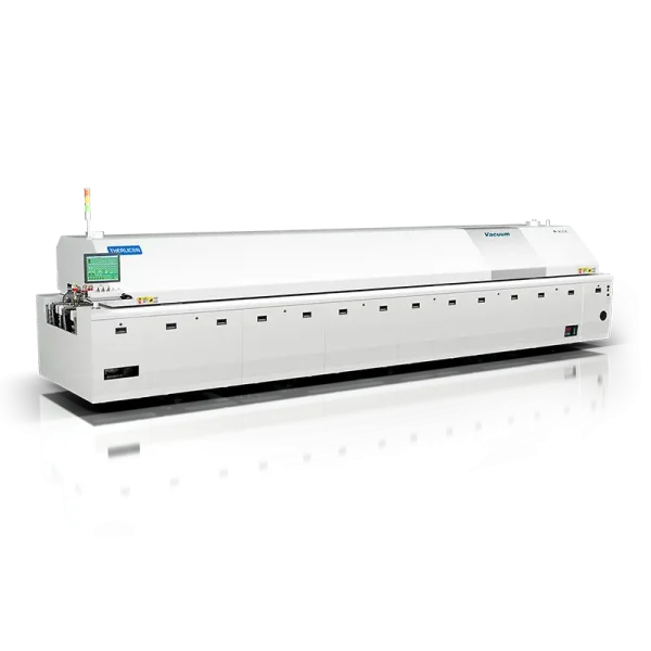

What temperature is used in reflow soldering?
Reflow soldering typically uses peak temperatures of around 210–230°C for leaded solder and 235–245°C for lead-free solder.
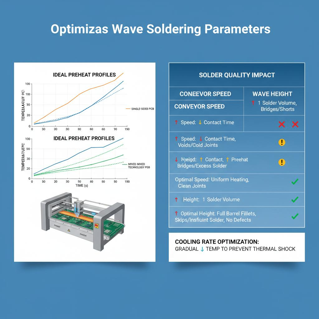
In reflow soldering temperature control in PCB manufacturing , the exact profile depends on the solder alloy. Leaded solder melts at a lower temperature, so it requires a gentler thermal profile. Lead-free solder (such as SAC alloys) needs higher peak temperatures to fully melt and form reliable joints.
For example, in modern SMT production lines for smartphones and laptops, lead-free profiles are standard due to environmental regulations, requiring tighter process control to avoid component damage while still achieving full solder wetting.
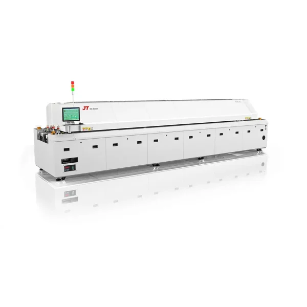
Can reflow soldering damage sensitive electronic components?
Yes, reflow soldering can damage sensitive components if temperature, time, or heating rate is not properly controlled.
In PCB reflow soldering risk management , common risk factors include excessive peak temperature, rapid heating (thermal shock), and long exposure time in the oven. These conditions can cause IC delamination, capacitor cracking, or package warping.
To reduce risk, manufacturers use controlled reflow oven temperature profiles , pre-baking sensitive components, and carefully tuning ramp-up rates. For example, ceramic capacitors in mobile devices are especially sensitive and require strict thermal control to prevent micro-cracks.
Why do reflow soldering defects occur even in automated production?
Reflow defects still occur due to process variation, material inconsistency, and equipment calibration drift, even in fully automated SMT lines.
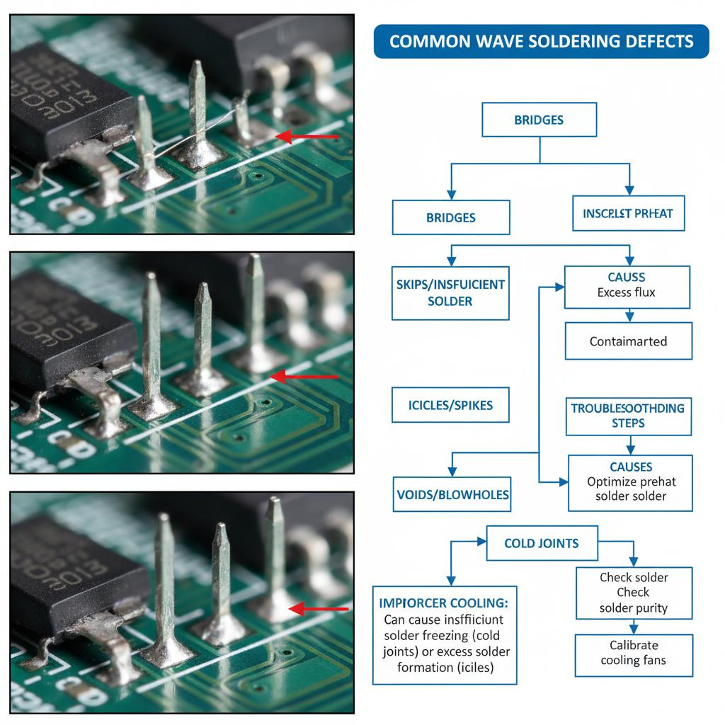
In automated SMT reflow production , machines reduce human error but cannot eliminate all variability. Small changes in solder paste viscosity, stencil wear, or component alignment can lead to defects.
Equipment calibration is another key factor. If the reflow oven temperature sensors are inaccurate, the actual thermal profile may differ from the programmed one, causing issues like cold joints or bridging.
For example, in high-volume PCB factories, periodic maintenance and process monitoring are required to keep defect rates low and ensure consistent output quality.
How is reflow soldering quality tested in PCB production?
Reflow soldering quality is tested using AOI, X-ray inspection, and electrical testing to detect visible and hidden defects.
In PCB quality control after reflow soldering , Automated Optical Inspection (AOI) is used to detect surface defects such as solder bridging, missing components, or misalignment.
For hidden joints like BGA packages, X-ray inspection is required to identify voids, cracks, or incomplete solder balls that cannot be seen visually. Electrical testing is then used to verify circuit continuity and functionality.
For example, in server and telecom boards, a combination of AOI and X-ray is mandatory to ensure zero-defect requirements before final shipment.
What industries rely most on reflow soldering technology?
Reflow soldering is widely used in industries that require high-density, reliable, and mass-produced electronic assemblies.
In SMT reflow soldering applications , the most dependent industries include consumer electronics (smartphones, laptops), automotive electronics (ECUs, sensors), medical devices (monitoring and diagnostic equipment), and industrial control systems.
These industries rely on reflow soldering because it provides consistent quality, high scalability, and suitability for miniaturized components used in modern PCB designs.
For example, automotive electronics require extremely stable solder joints due to vibration and temperature changes, while medical devices demand high reliability for safety-critical operation.