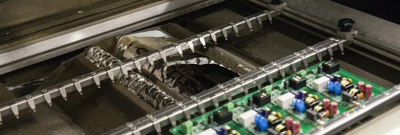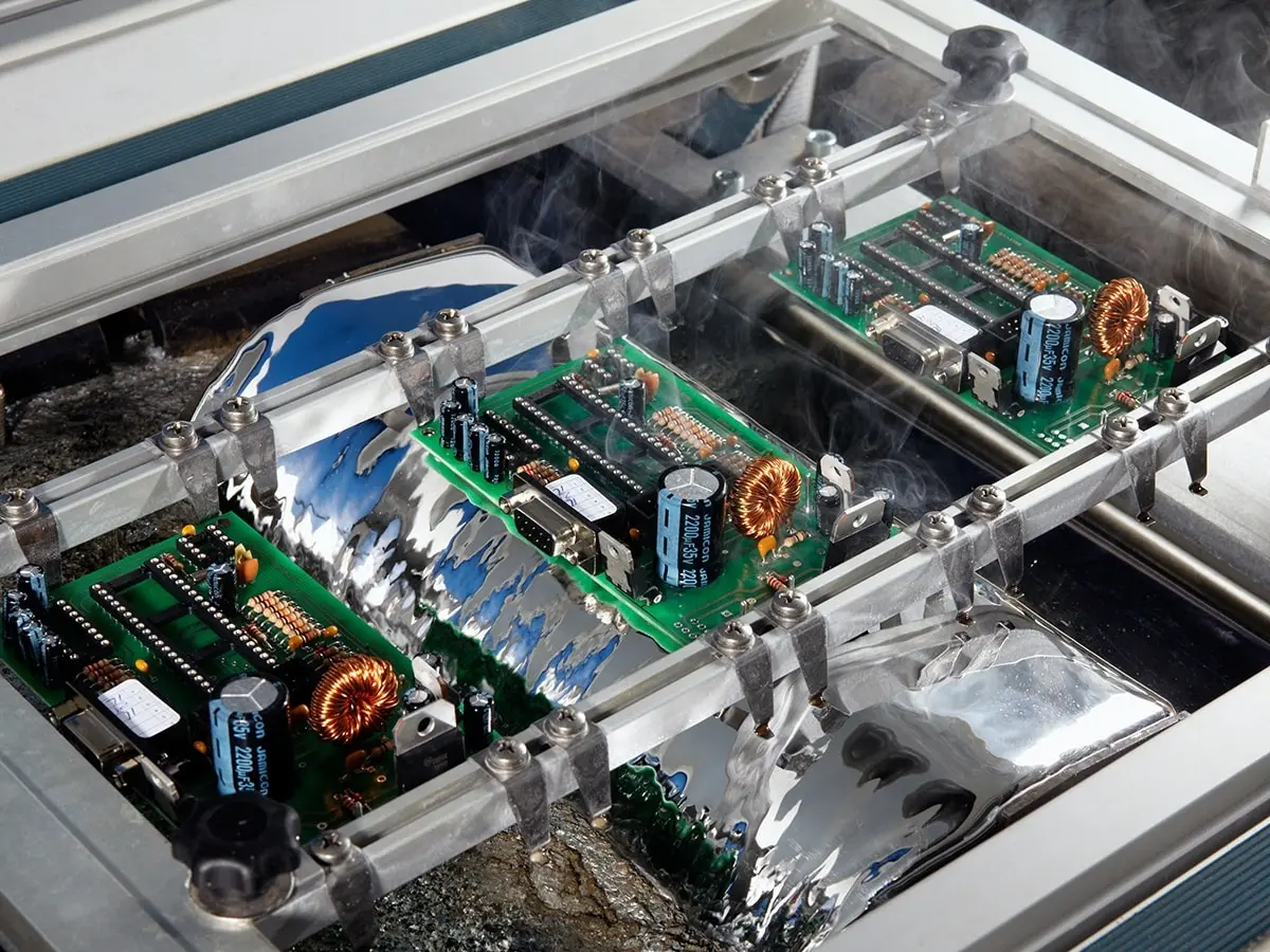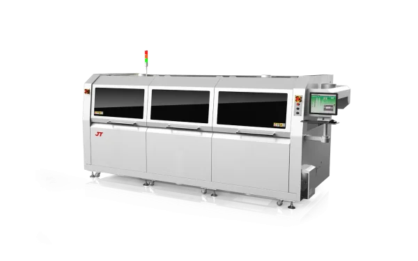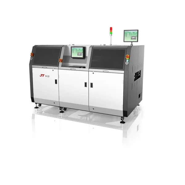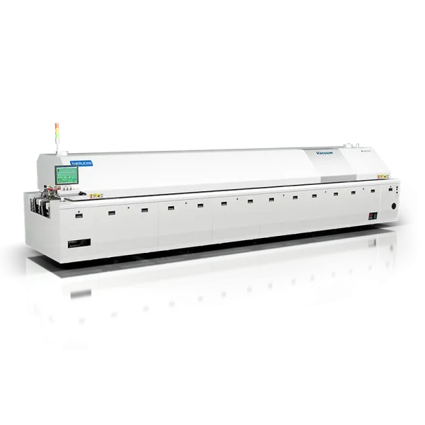

The reflow soldering process is the most important step in surface mount technology (SMT) assembly to mount surface mount devices (SMDs) onto a printed circuit board (PCB). Reflow soldering is a process where solder paste melts and forms permanent electrical and mechanical connections between the SMDs and the PCB’s copper pads. The success of reflow soldering relies on solder paste application, reflow profiling, and design for manufacturability (DFM).
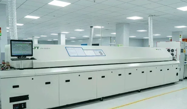
How to Ensure Reflow Soldering Success
Achieving consistent, zero-defect reflow soldering requires attention to detail in design, material handling, and process management. PCBONLINE has rich experience in PCB assembly, and we pay attention to every detail to provide a successful reflow soldering process.
1. Precise reflow profile
The temperatures in the reflow soldering process follow a reflow profile, which is the blueprint for a successful reflow.
Profile verification: Use a thermal profiler with thermocouples to attach directly to the PCB to map the actual temperatures experienced by various points on the PCB, especially near large components.
Zone tuning: Adjust the heater settings and conveyor speed until the measured profile strictly complies with the specifications of the solder paste and the most sensitive components.
Oxygen control (nitrogen reflow): For highly demanding applications, using a nitrogen atmosphere (keeping O2 < 500ppm) improves flux activity, enhances wetting, and minimizes oxidation, resulting in brighter, stronger solder joints.
2. Design for manufacturability (DFM) rules
Good PCB layout design is the first defense against defects. PCBONLINE offers a free and professional DFM before PCB prototype production.
Every incoming component undergoes strict inspection, including visual and microscopic inspection, electrical verification, and batch traceability.
Component orientation: Small and chip-style components, especially 01005, 0402, and 0603, should have their long axis positioned parallel to the reflow oven conveyor direction. Keeping the small SMD orientation parallel with the flow conveyor direction minimizes the risk of Tombstoning, a PCB soldering defect where the component stands up on one end. This is because it provides maximum surface tension stabilization against minor air currents.
PCB orientation: The long axis of the PCBs penalized in a production panel should also be positioned parallel to the conveyor direction. It ensures maximum thermal uniformity across the PCB surface as it passes through the heating zones.
Thermal relief: Pads connected to large copper planes, like power and ground pour,s must use thermal relief spokes. It prevents the heat from being excessively drawn away from the pad, which causes cold solder joints or non-wetting issues.
Pad geometry: Ensure symmetry in the size and shape of corresponding pads, for example, both ends of a resistor. Asymmetrical pads cause uneven solder paste melting and surface tension forces, leading to component skewing.
3. Material quality control
We have strict quality control over the materials used for the reflow soldering process, including solder paste management and handling sensitive components.
Solder paste management: Solder paste must be stored under refrigeration and allowed to warm up to ambient temperature before use. At PCBONLINE, we’ve upgraded to a smart solder paste management cabinet, which automatically stores, warms up, and records the solder paste for traceability. Failure to properly acclimate the paste can lead to moisture condensation, resulting in excessive solder balls and splattering during reflow.
Handling moisture-sensitive devices: We handle components designated as Moisture Sensitivity Level (MSL) 2 or higher according to J-STD-033. If they have exceeded their floor life, they must be baked before reflow to prevent internal moisture from expanding or even popcorning during the reflow process.
4. SMT stencil design
Precise solder paste printing heavily depends on the SMT stencil design. PCBONLINE has rich experience in SMT stencil design to ensure precise solder paste deposition onto the PCB copper pads. Most openings are designed 1:1 to the copper pads, but for ultra-small components, fine-pitch ICs, etc, we need to design their corresponding openings in the SMT stencil specially.
For stencil openings corresponding to fine-pitch ICs and QFPs, we design the two ends of the aperture with rounded corners.
For BGAs and ultra-small SMDs like 0402 and 0201, we design their stencil openings square-shaped.
For stencil openings corresponding to QFN ground pads in a cross-shape (“+”), we ensure at least 0.5 mm clearance from the PCB pad edge.
For USB, Mini USB, and CF/SD connectors, we extend the length in a 1:1.2 ratio to increase solder volume. To reduce stress and prevent solder beads, we use an inward concave opening method.
We ensure enough stencil opening width to allow at least four solder balls to pass through.
5.Dual-AOI to ensure reflow soldering success
each of our SMT lines is equipped with two in-line AOI machines, before and after the reflow soldering process.
Both are three-dimensional optical inspections. The prior-reflow AOI checks the component placement and ensures no potential risks of tombstoning before reflow. The post-reflow AOI checks the PCBA surface to ensure no soldering defects after the reflow soldering process.
6. Nitrogen reflow soldering
Last but not least, if the PCBA is double-sided and easy to oxidize during reflow soldering, we can also provide nitrogen reflow to replace standard reflow soldering.