
SMT assembly process is fully automated and precise. We ensure efficient and high-quality PCB production. The steps of the SMT surface mount technology process are below.
Loading bare PCBs
The process starts by loading bare PCBs onto the SMT production line. A dedicated loader machine feeds individual PCBs automatically. This ensures a continuous flow.
Solder paste printing
Next, the PCB moves to the solder paste printing station. A vision system precisely aligns the PCB under an SMT stencil. A squeegee then moves across the stencil. It presses a precise amount of solder paste through the stencil’s openings. This paste goes onto the designated pads on the PCB surface. Solder paste is a sticky mix of tiny solder particles and flux. It acts as a temporary adhesive and forms a strong electrical connection. The squeegee’s controlled speed, pressure, and angle are vital for consistent application.
Solder paste inspection (SPI)
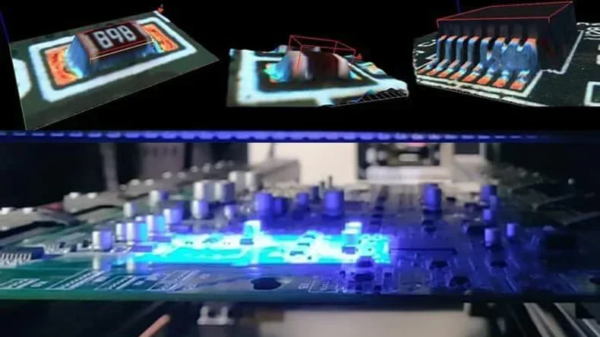
After printing, the PCB undergoes Solder Paste Inspection (SPI). A 3D SPI machine scans the applied solder paste using an infrared camera. This inspection verifies the paste’s position, shape, and thickness against quality standards. Deviations are caught early. This prevents costly rework later in the process.
Pick-and-place of SMDs
Following a successful SPI, the PCB goes to the pick-and-place stage. High-speed, automated machines use vacuum nozzles or grippers. They accurately pick individual Surface Mount Devices (SMDs) from feeders. Advanced vision systems then precisely place each component. It goes onto its corresponding solder-pasted pads on the PCB. Modern pick-and-place machines can place tens of thousands of components per hour. This highlights SMT’s incredible efficiency.
Automated optical inspection (AOI) before reflow soldering
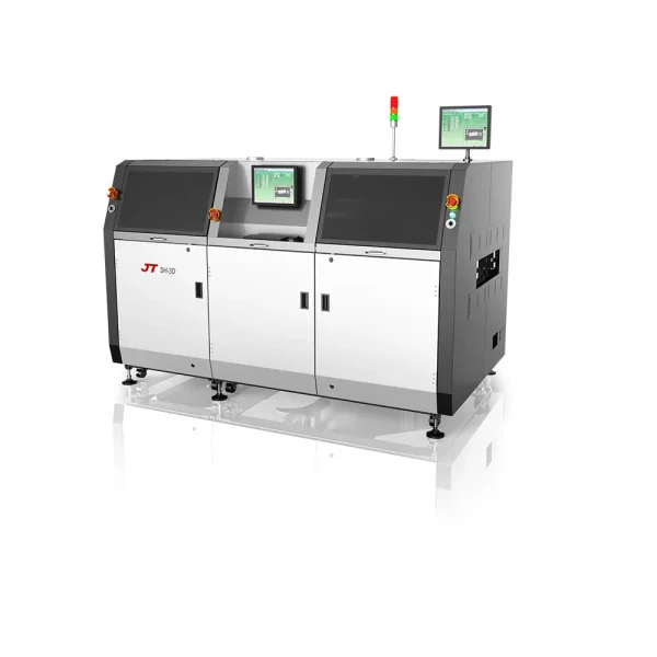
Before reflow soldering, another critical inspection occurs. A 3D Automated Optical Inspection (AOI) machine is used. This AOI checks the populated PCBA for placement issues. It looks for missing components, misalignment, or incorrect polarity. Catching these errors early allows for immediate correction. This prevents permanently flawed assemblies.
Reflow soldering
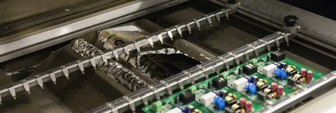
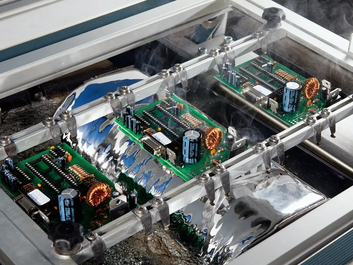
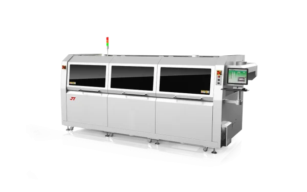
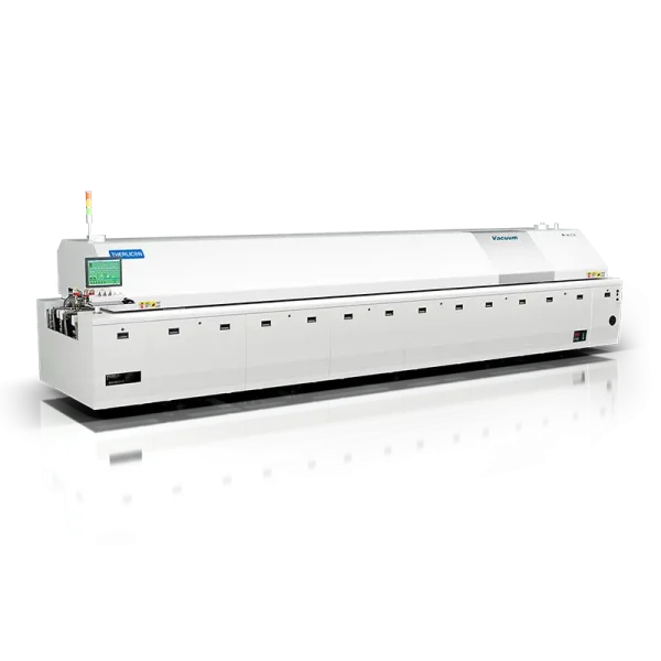
The PCBA then enters a reflow oven. This is typically a lead-free oven with multiple temperature zones. As the board moves through these zones, it undergoes a careful heating profile. The solder paste first melts (reflows). The molten solder then creates strong metallurgical bonds between the SMD leads/pads and the PCB pads. The molten solder’s surface tension helps self-align components. Finally, the board cools. The solder solidifies, forming permanent electrical and mechanical connections.
Automated optical inspection (AOI) after reflow
The final major step is AOI after reflow. A 3D AOI machine performs a full scan of the soldered board. It ensures soldering quality and component placement accuracy. This inspection checks for common defects. These include solder bridging, tombstoning, and irregular solder joint shapes. This final quality check ensures the assembled PCB meets strict standards.