
Visual Inspection: Visual inspection is a critical step in the surface mount soldering quality control process. It involves inspecting solder joints and components on the circuit board to identify defects or anomalies that may affect the performance and reliability of the assembled electronic equipment. Visual inspection can be performed manually or with the aid of an Automated Optical Inspection (AOI) system.
Manual Visual Inspection: Manual visual inspection refers to operators carefully inspecting the printed circuit board (PCB) under a magnifying glass to identify potential defects. This method allows for human judgment of whether solder joints are acceptable or require rework. However, manual inspection is time-consuming and prone to human error. Tutorials indicate that skilled operators must ensure the consistency and accuracy of inspection results.
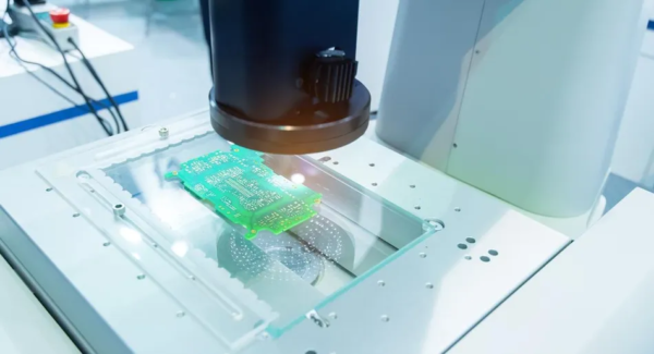
Automated Optical Inspection (AOI): AOI systems use cameras, lighting equipment, and image processing software to automatically detect defects on PCBs. The AOI system compares the acquired images to predefined standards to identify anomalies. Compared to manual inspection, AOI offers several advantages, including higher speed, accuracy, and repeatability. AOI systems can detect a variety of defects, such as solder bridges, component misalignment, and insufficient solder.
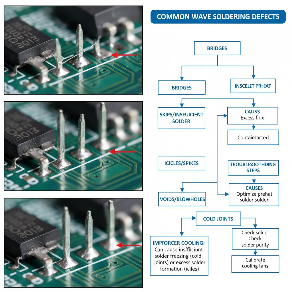
Defect Detection: Visual inspection, whether manual or automated, aims to identify various types of soldering defects, such as:
Solder Bridges: Unexpected connections between solder joints can cause short circuits.
Insufficient Solder: Insufficient solder on solder joints leads to unstable mechanical and electrical connections.
Excessive Solder: Too much solder on solder joints can cause short circuits or affect the performance of nearby components.
Component Misalignment: Improper placement of components can lead to poor electrical connections or subject solder joints to mechanical stress.
Post-Inspection Actions: After visual inspection, all defects found must be addressed. Rework may be required to correct identified problems, such as desoldering and resoldering components or removing excess solder. Recording inspection results and all rework actions is crucial for maintaining traceability and improving process control.
In summary, visual inspection is essential for ensuring the quality and reliability of surface mount soldering. By employing manual or automated techniques, manufacturers can detect and resolve soldering defects, thereby improving the performance and lifespan of electronic products.
X-ray Inspection
Inspection and Quality Control
X-ray inspection is a non-destructive testing method used to assess solder joint quality and detect hidden defects in surface mount soldering. This technology is particularly suitable for inspecting solder joints beneath components with limited or no optical accessibility, such as Ball Grid Arrays (BGAs) and Quad Flat No-Leader (QFN) packages.
X-ray Inspection Process: X-ray inspection systems generate X-rays that pass through the PCB and are captured by a detector, creating a radiographic image of the internal structure of the solder joint. The image contrast depends on the differences in X-ray absorption by different materials; denser materials (such as metals) appear brighter in the image. Operators or automated image processing software analyze these images to identify potential defects.
Defect Detection: X-ray inspection is particularly effective for detecting defects that are difficult or impossible to identify using visual inspection methods. These defects include:
Voids: Air bubbles or gaps inside a solder joint can affect its mechanical and thermal properties. X-ray inspection can reveal the size, shape, and location of voids, allowing manufacturers to assess their impact on solder joint integrity.
Bridging: X-ray inspection can identify solder bridging beneath surface-mount components, which visual inspection cannot.
Insufficient or Excessive Solder: X-ray images can reveal the amount of solder in hidden solder joints, helping to identify insufficient or excessive wave soldering that may affect solder joint performance.
Limitations of X-ray Inspection: While X-ray inspection is a powerful tool, it also has some limitations:
False Positives and False Negatives: X-ray images can produce false positives or false negatives in defect identification. To minimize this risk, careful analysis and comparison with other inspection methods are essential.
Material Limitations: X-ray inspection may be less effective with materials having similar X-ray absorption characteristics, making it difficult to distinguish them in the captured images.
Complementary Inspection Techniques: X-ray inspection should be used in conjunction with other inspection methods, such as visual inspection and automated optical inspection, to ensure comprehensive defect detection and quality control. By combining multiple inspection techniques, manufacturers can more effectively identify and address potential problems, thereby improving product reliability and performance.
Automated Optical Inspection (AOI)
Automated Optical Inspection (AOI) is a non-contact, high-speed inspection method widely used in the electronics manufacturing industry to ensure the quality of printed circuit board (PCB) assemblies. AOI systems utilize cameras and image processing software to automatically inspect PCBs and compare them to predefined standards, thereby identifying defects or deviations from reference designs.
AOI System Components: AOI systems typically consist of several key components:
High-Resolution Camera: AOI systems use one or more cameras to capture high-resolution images of the PCB surface. Depending on the system configuration, cameras can be placed at different angles to inspect the board from various perspectives, thus improving defect detection rates.
Illumination: Uniform and stable illumination is crucial for accurate imaging. AOI systems typically use a variety of light sources with different wavelengths and angles to produce the required contrast and minimize shadows.
Image Processing Software: This software processes the acquired images and compares them to reference images or design data to identify potential defects. Advanced AOI systems employ machine learning algorithms to improve inspection accuracy and adapt to variations in component appearance and solder joint quality.
Defect Detection: AOI systems can detect a variety of defects, including:
Component Presence, Orientation, and Alignment: AOI systems can verify the presence, correct orientation, and precise alignment of all components on the PCB with their respective pads.
Solder Joint Quality: By analyzing the shape, size, and color of solder joints, AOI systems can identify soldering defects such as insufficient or excessive solder, bridging, and poor wetting.
Component Polarity: AOI systems can verify that components are mounted in the correct orientation to meet specific polarity requirements, thus preventing potential failures or damage.
Inspection Speed and Accuracy: One of the main advantages of AOI systems is their speed, capable of inspecting thousands of components per hour, far faster than manual inspection methods. The accuracy of AOI systems depends on various factors, such as camera resolution, lighting conditions, and image processing algorithms. Typical AOI systems achieve a defect detection rate of 90% or higher, with a false alarm rate of less than 10%.
Limitations of AOI: While AOI is a powerful inspection method, it also has some limitations:
Hidden Solder Joints: AOI systems cannot inspect solder joints that are not visible beneath SMD components (such as BGAs or QFNs) due to the lack of optical channels. X-ray inspection is required to assess the quality of these hidden solder joints.
Component Appearance Variations: Variations in component appearance due to manufacturing tolerances or component supplier changes can pose challenges to automated inspection systems, potentially leading to false alarms or missed defects. Regular system calibration and training help mitigate this issue.
Integration with Other Inspection Methods: AOI is an important component of a comprehensive inspection strategy and can complement other inspection methods such as visual inspection, X-ray inspection, and functional testing. By integrating multiple inspection technologies, manufacturers can more effectively identify and resolve potential problems, thereby improving the overall quality and reliability of their products.
Conclusion: In the electronics manufacturing industry, reflow soldering processes are crucial for ensuring the reliability and high quality of PCB components. Inspection and quality control technologies are essential for verifying solder joint quality and identifying potential problems before they affect the performance of the final product. By integrating these concepts and methods, manufacturers can improve the efficiency, yield, and product reliability of their electronics manufacturing processes.