In the PCB assembly chain of electronics manufacturing, wave soldering technology, with its proven batch soldering capabilities, has become a core support for through-hole soldering (THT) and hybrid process production. From home appliances to automotive electronics, this technology, through standardized processes and precise control, ensures the stable operation of electronic devices. Its deep adaptation of principles and application scenarios further demonstrates the refined development of industrial manufacturing.
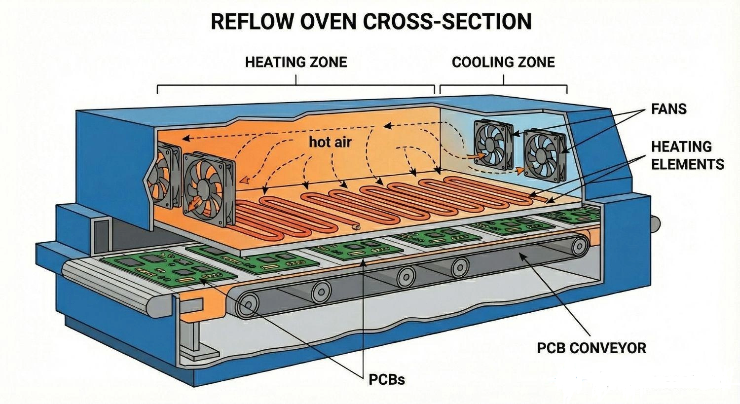
The core operating principle of wave soldering is to use a mechanical or electromagnetic pump to form a stable wave of molten solder, ensuring full contact between the soldering surface of the PCB and the liquid solder to achieve a connection. The complete process involves five key steps:
1. First, the PCB with embedded components is transported to the equipment via a transmission system.
2. Flux is then evenly applied through a spray device to prevent solder oxidation.
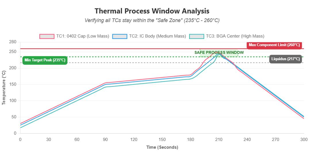
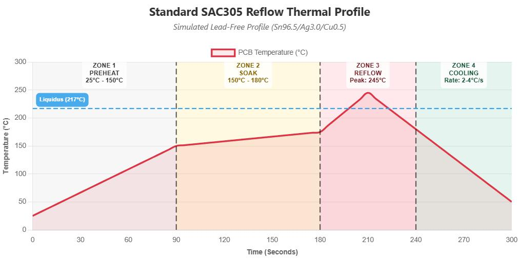
3. After entering the preheating zone, the PCB temperature gradually rises to 90-100°C, activating the flux and preventing subsequent thermal shock.
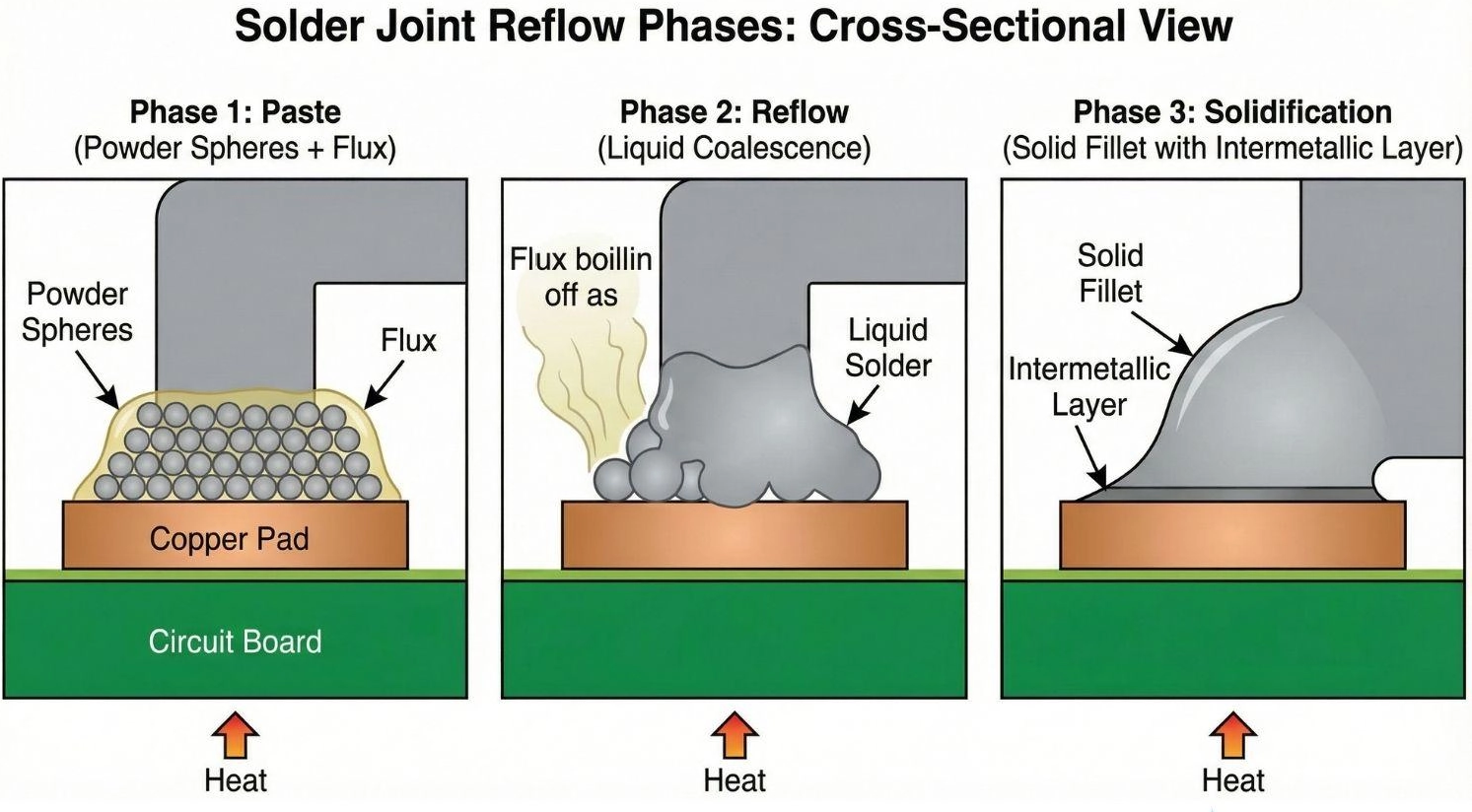
4. During the core soldering phase, the PCB is immersed in a 220-240°C molten tin bath using a single or dual-wave soldering process. The dual-wave design allows for the perturbation wave to penetrate densely packed pins, while the lambda wave forms the solder joints.
5. Finally, the solder joints are solidified through a cooling system, forming a reliable mechanical and electrical connection.
With increasing environmental protection requirements, lead-free processes have become mainstream. Tin-silver-copper alloys are being used to replace traditional lead-tin alloys. While this increases the preheating temperature, it also achieves environmentally friendly production.
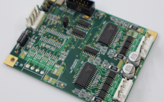
The application scenarios of wave soldering have continued to expand with technological iterations, resulting in distinct differentiation. In the consumer electronics sector, traditional wave soldering is commonly used for efficient mass production of single-sided or regularly laid PCBs for products such as televisions and digital set-top boxes. Its low cost advantage makes it suitable for large-scale manufacturing.
Traditional wave soldering is a typical application for devices like home appliance control boards and switching power supplies, due to their densely packed components. This significantly improves production efficiency and reduces costs.
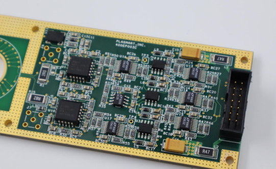
In high-end sectors like automotive electronics and medical electronics, high-density PCBs with mixed double-sided SMD and plug-in components require stringent soldering precision. Selective wave soldering, which uses specialized nozzles to precisely solder designated areas, effectively protects sensitive components from damage, making it the preferred solution for these applications.
In addition, PCB assembly for industrial equipment such as outdoor LED lights also relies on wave soldering technology to achieve stable and reliable soldering results.
From traditional mass production to high-end precision soldering, the development of wave soldering technology has consistently responded to the evolving needs of electronics manufacturing. Throughout this process, Jintuo, leveraging its deep understanding of process details and technological innovation, has provided customized solutions for diverse applications, from large-scale production of consumer electronics to precision soldering for high-end manufacturing, continuously driving the high-quality development of the electronics industry.