In the printed circuit board (PCB) assembly process, wave soldering plays a crucial role in component fixation. With continuous upgrades in manufacturing technology and increasing environmental awareness, wave soldering has been further subdivided into leaded wave soldering and lead-free wave soldering. To ensure optimal quality, the differences in manufacturing processes inevitably lead to different applications. Therefore, understanding the differences between the soldering techniques used in leaded and lead-free wave soldering is essential.

Solder Content Comparison
• Commonly used solders in wave soldering are:
a. Eutectic solder: Sn37Pb. It is a single homogeneous solder with a melting point of 183℃, composed of two phases (Sn and Pb) with different melting points.
b. Solder: Sn36Pb2Ag. Adding a small amount of Ag to SnPb solder serves two purposes:
Purpose 1: Lowering the melting point of the solder (e.g., Sn36Pb2Ag has a melting point of 179℃), improving diffusion and solder strength, and resulting in a bright and aesthetically pleasing solder joint. This solder is suitable for quartz crystal units, ceramic devices, thermistors, thick-film devices, integrated circuits (ICs), and silver-plated components.
Purpose Two: To prevent the solder and Ag from interdiffusion on the substrate, Ag needs to be added to the solder beforehand. This prevents Ag diffusion on ceramics and mica, and the Ag layer will not peel off; this is the main application characteristic of this solder.
• Commonly used solders in lead-free wave soldering are:
a. Alloy Sn3.0Ag0.5Cu (SAC305). It is one of the most widely used elements in the industrial field, with a melting point range of 217℃ to 220℃. Sn3.8Ag0.7Cu (SAC387) is a single-crystal element of SnAgCu alloy, with a melting point of 217℃.
b. Alloy Sn0.7Cu. As a single-crystal element in the SnCu series alloys, Sn0.7Cu has a melting point of 227℃, which is 9℃ higher than SAC305. Therefore, it is no longer suitable for reflow soldering when the soldering temperature exceeds 250℃.
Wave Soldering Process Window
• Wave Soldering
a. Regarding Sn37Pb eutectic solder:
1) Wave Soldering Temperature. For Sn37Pb eutectic alloys, the soldering temperature should be 37℃ higher than the melting point. Therefore, the theoretical soldering temperature is 220℃ (183℃ + 37℃).
During wave soldering, the solder temperature is not equivalent to the solder bath temperature. The solder melting temperature is the intermediate temperature between the solder bath temperature and the workpiece operating temperature. To ensure good wettability of the solder, after reaching the minimum wetting temperature, the solder bath temperature needs to be further increased to approximately 250℃ to compensate for other heat losses, thereby achieving thermal equilibrium during wave soldering.
2) Wave Soldering Time. For optimal wave soldering results, the solder joint should be immersed in the wave solder for 2 to 4 seconds.
b. For Sn36Pb2Ag solder, the wave soldering process window can be set with reference to Sn37Pb solder.
• Lead-free Wave Soldering
Temperature selection for lead-free wave soldering is an important method to overcome insufficient wettability of lead-free solders. Based on the optimal wettability temperature range for wave soldering, a temperature typically selected is 50°C higher than the highest melting point. Therefore, the commonly used lead-free solder process windows for obtaining optimal wettability are as follows:
a. For SAC305 soldering:
1) Wave soldering temperature: 250°C to 260°C;
2) Wave soldering time: Recommended time is 3 to 5 seconds.
b. For Sn0.7Cu alloy:
1) Wave soldering temperature: 260°C to 270°C;
2) Wave soldering time: Comparable to SAC305 alloy.
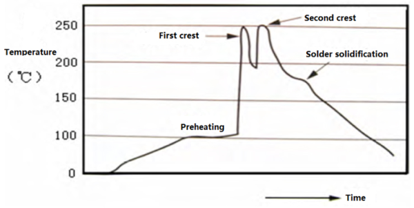
Wave Soldering Time-Temperature Profile
The main process parameters for wave soldering technology are concentrated in the time-temperature profile.
• Wave Soldering
The figure below shows the time-temperature profile for wave soldering using Sn37Pb solder.
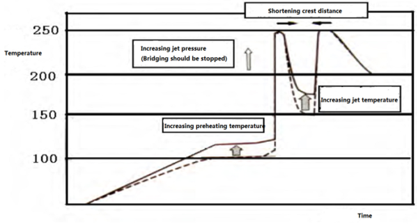
• Lead-free wave soldering
Because lead-free solders (such as SAC305) have poorer wettability than Sn37Pb, through-hole defects are easily generated when wave soldering through-hole components. Therefore, some modifications to the time-temperature profile of lead-free wave soldering are required, as shown in the figure below.
Copper Impurity Control in Wave Soldering
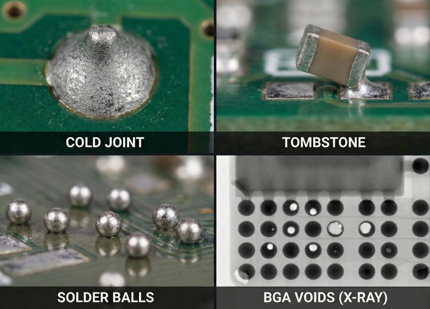
In wave soldering, a change of 0.2% (wt%) in copper content in the solder bath results in a maximum change of 6°C in the liquid phase temperature. Such a large change leads to significant differences in the properties of the liquid solder, resulting in decreased solder flowability, impaired mechanical properties of the wave soldering process, and soldering defects such as bridging. Therefore, controlling the copper content in the solder bath is crucial.
Copper control in the wave soldering bath is based on the following two physical phenomena:
a. Density difference. After copper melts in the solder bath, it exists as a Cu₆Sn₅ metallic compound. Since the density of Sn₃₇Pb is 8.5 g/cm³, while the density of Cu₆Sn₅ is 8.3 g/cm³, the latter floats on the surface of the liquid Sn₃₇Pb in the solder bath. b. Melting point difference. The melting point of Cu₆Sn₅ is 5–10°C higher than that of Sn₃₇Pb and also 5–10°C higher than that of SnPb. Therefore, the solder bath temperature can be lowered below the melting point of Cu₆Sn₅, and then the copper-tin alloy can be picked out and removed using a special tool. Finally, the solder bath is replenished with high-purity environmentally friendly solder.
In lead-free wave soldering, it is recommended to upgrade the solder when the copper impurity content in the solder bath reaches 1.55 (wt)%. This is because once this value is exceeded, the wettability of most lead-free alloys decreases sharply. a. In the case of lead-free wave soldering, the SnCu compound Cu₆Sn₅, with a density of 8.3 g/cm³, is higher than SnAgCu and SnCu, causing the SnCu compound Cu₆Sn₅ to be unable to float in the liquid solder, resulting in numerous soldering defects. b. In the case of lead-free wave soldering, when the rate at which copper melts into the solder bath cancels out the rate at which copper is removed from the solder bath by the PCB, and is diluted by the newly added solder, the copper content in the solder bath will reach a dynamic equilibrium. At this point, soldering must be carried out immediately under nitrogen protection.