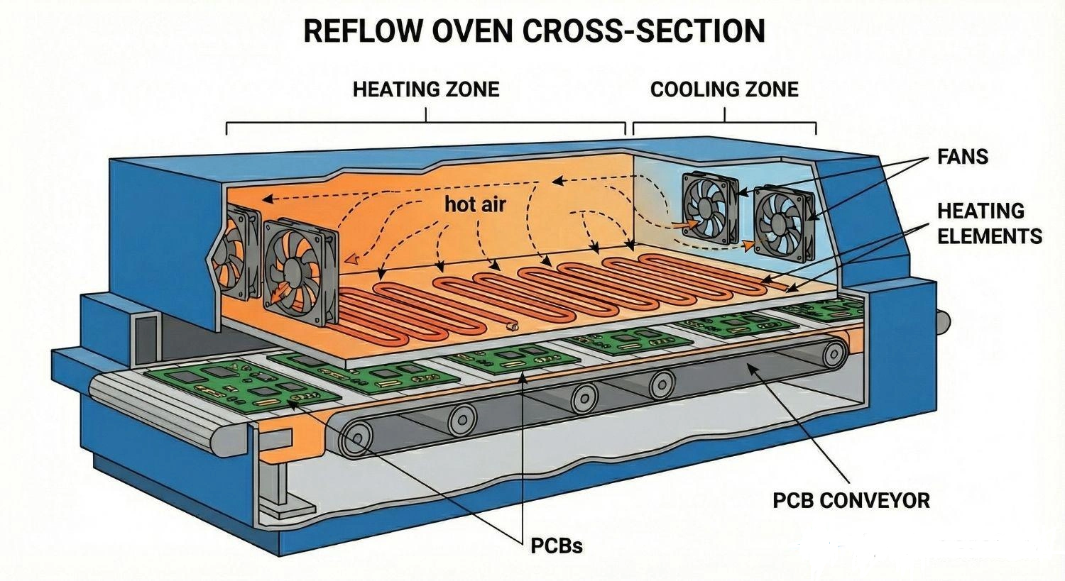
The reflow soldering process in PCB manufacturing works by printing solder paste, placing components, and then passing the board through a controlled multi-stage heating cycle (preheat, soak, peak reflow, and cooling) that melts and solidifies the solder to form reliable electrical and mechanical connections.

Step 1 — Solder paste printing on PCB pads
Solder paste printing is the process of applying a precise amount of solder paste onto PCB pads using a stencil before components are placed.
In SMT reflow soldering, the process starts with solder paste printing in PCB manufacturing, where a stainless-steel stencil is aligned over the PCB. A squeegee blade then spreads solder paste across the stencil openings so it deposits only on the required pads.
The key factor here is paste deposition control in PCB assembly. If too much solder paste is applied, it can cause solder bridges after reflow. If too little is applied, the joint may become weak or fail electrically.
For example, in smartphone PCB production, even a 0.1 mm variation in paste volume can affect signal stability. That is why factories tightly control stencil thickness, paste viscosity, and printing pressure.
Step 2 — SMT component placement before reflow
Component placement is the process where machines accurately position electronic parts onto solder-pasted pads before heating.
After printing, a pick-and-place machine in SMT assembly places components directly onto the solder paste. These machines use vacuum nozzles and vision systems to achieve extremely high precision.
The most important requirement is placement accuracy in PCB manufacturing, especially for fine-pitch ICs and micro components. Even a small offset can cause poor solder joints or short circuits after reflow.
For example, in an HDI PCB used in a laptop motherboard, components are placed with micron-level accuracy so they perfectly align with solder paste deposits. The sticky nature of solder paste helps hold components temporarily before they enter the oven.
Step 3 — Preheat zone in reflow oven
The preheat zone gradually increases PCB temperature to prevent thermal shock and prepare solder paste for reflow.
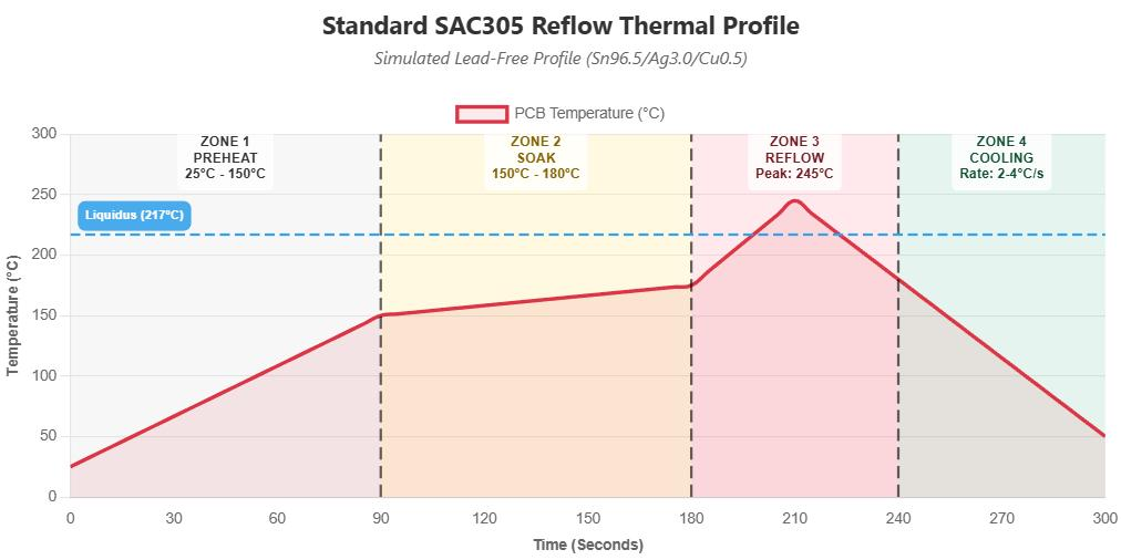
In the reflow soldering preheat stage, the PCB enters a controlled heating zone where temperature rises slowly. This is important to avoid thermal shock in PCB components, which can crack sensitive parts.
During this stage, the flux inside the solder paste begins to activate, and solvents start to evaporate. This helps clean oxidation from metal surfaces and prepares them for strong bonding later.
For example, if a PCB is heated too quickly (like placing it directly into high heat), ceramic capacitors may crack. That is why reflow ovens use a controlled ramp-up profile.
Step 4 — Soak zone for thermal stabilization
The soak zone ensures the entire PCB reaches a uniform temperature and activates flux for better soldering quality.
In the soak phase of reflow soldering, the PCB temperature is held steady for a short time. This allows different areas of the board—thick and thin sections—to equalize in temperature.
This step is important for thermal balance in PCB reflow process, especially for large multilayer boards where heat spreads unevenly.
At the same time, the flux becomes fully active and removes oxidation from copper pads and component leads, improving solder wetting during the next stage.
For example, in automotive PCBs, soak control is critical because uneven heating can lead to unreliable solder joints under vibration conditions.
Step 5 — Reflow (peak temperature zone)
The reflow zone is where solder melts, flows, and forms strong electrical and mechanical connections.
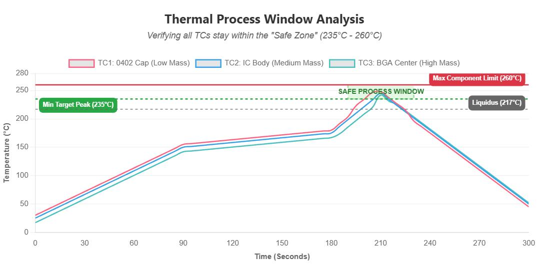
During the peak reflow stage in SMT soldering, the temperature reaches the melting point of solder (typically 217°C–245°C for lead-free solder). The solder paste becomes liquid and flows around pads and component leads.
This process creates solder wetting in PCB assembly, where molten solder spreads evenly and forms a strong bond.
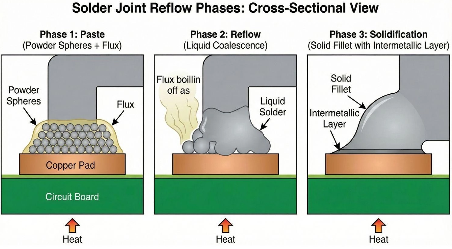
At this stage, intermetallic compounds (IMC) formation in solder joints occurs. These IMCs are essential because they create a strong metallurgical connection between copper and solder.
For example, in a fine-pitch QFN chip, proper peak temperature ensures all pins form uniform joints without voids or weak connections.
Step 6 — Cooling zone and solidification
The cooling zone solidifies solder joints in a controlled way to ensure strength and prevent defects.
In the cooling stage of reflow soldering, the PCB temperature is reduced in a controlled manner. This prevents thermal stress and helps solder solidify evenly.
A proper cooling rate is critical for reflow solder joint reliability, because cooling too fast can cause cracks, while cooling too slow can lead to weak grain structures.
For example, in high-reliability aerospace electronics, controlled cooling is used to ensure solder joints can withstand vibration and temperature cycling over long periods.
At the end of this stage, all components are permanently fixed, forming strong electrical paths and mechanically stable joints across the entire PCB.