AOI is a critical quality control technology in modern manufacturing, widely used for non-contact inspection of products in industries like electronics (PCB/SMT), automotive, semiconductor, and pharmaceuticals. Its core principle is to automatically identify surface defects by capturing images of an object and analyzing them through advanced image processing and algorithms.
1. Core System Components
-
Imaging System:
-
Lighting & Illumination: The most crucial element. Strategically designed light sources (e.g., LED ring lights, coaxial lights, backlights, dome lights) highlight specific features (solder joints, textures, contours) and suppress noise. Different lighting schemes reveal different defects.
-
Image Acquisition: Consists of high-resolution industrial cameras (CCD or CMOS) and lenses that convert optical signals into digital image data. Line-scan or area-scan cameras are chosen based on application needs.
-
-
Motion Control System:
-
Precisely controls the movement of the camera and/or the object under inspection (via XY stages, conveyors, or robots) to ensure complete coverage of the target area.
-
-
Image Processing & Analysis System (The “Brain”):
-
Computer & Processing Hardware: Hosts powerful image processing software and algorithm libraries, often accelerated by GPUs.
-
Software Algorithms: Executes the core inspection logic, ranging from traditional rule-based methods to modern AI-driven approaches.
-
2. Core Working Principle & Process Flow
Step 1: Image Acquisition
The system captures high-resolution digital images of the product under consistent, optimized lighting conditions as it moves through the inspection station.
Step 2: Image Pre-processing
Raw images are enhanced to improve analysis accuracy. Common operations include:
-
Noise reduction
-
Contrast enhancement
-
Geometric and color calibration
Step 3: Feature Extraction & Algorithm Analysis (The Core)
This step compares the processed image against a “standard.” Two primary technological approaches are used:
-
Traditional Rule-Based / Template Matching:
-
Template/Learning Phase: A “golden sample” (known good product) or CAD data is used to create a reference template, defining correct features (location, size, grayscale value, shape).
-
Comparison: The runtime image is compared pixel-by-pixel or feature-by-feature to this template.
-
Deviation Detection: Differences (e.g., brightness deviation, positional offset, area change) are calculated. If deviations exceed predefined thresholds, a defect is flagged.
-
-
Modern Deep Learning-Based Approach:
-
Model Training: A deep learning model (typically a Convolutional Neural Network – CNN) is trained on thousands of labeled images containing both “good” units and various defect types.
-
Intelligent Inference: The trained model autonomously learns the abstract characteristics of defects. For a new image, it can classify and locate anomalies (e.g., “missing component,” “scratch,” “contamination”) with high accuracy.
-
Advantage: Excellent for complex, variable, or undefined defects; reduces false calls; requires less precise programming; adapts well to new products.
-
Step 4: Defect Decision & Classification
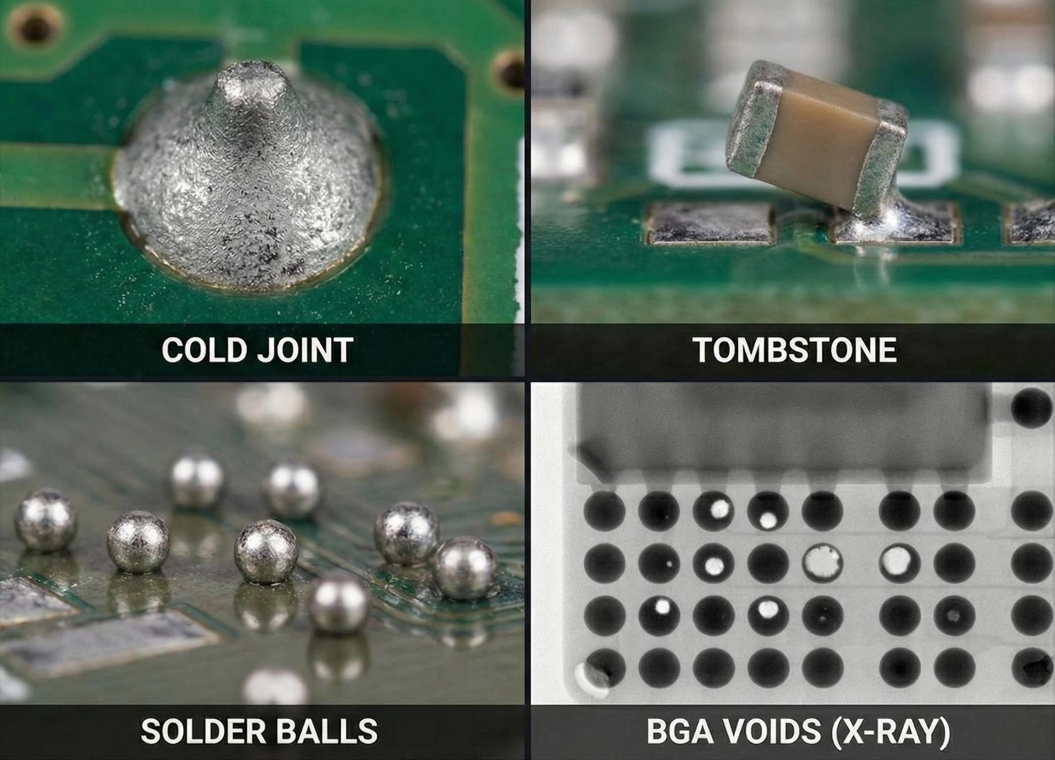
Based on the algorithm’s output, the system automatically classifies each inspected area as “PASS” or “FAIL” according to configurable criteria. Failures are categorized (e.g., solder bridge, tombstones, marking error) and their precise coordinates are logged.
Step 5: Result Output & Action
-
Data Output: Generates detailed inspection reports with defect maps, statistics, and trend analysis.
-
Real-time Action: Triggers alarms, marks the defective product, or communicates with other machines (e.g., via PLC I/O or SECS/GEM protocol) to reject the unit from the production line.
3. Key Technical Characteristics
-
High Speed & Accuracy: Achieves micron-level resolution at production line speeds.
-
Repeatability & Reliability: Provides consistent, objective inspection 24/7, eliminating human fatigue and subjectivity.
-
Flexibility: Inspection programs can be quickly changed for different products.
-
Data-Driven Manufacturing: Provides traceable quality data for process optimization and yield improvement.
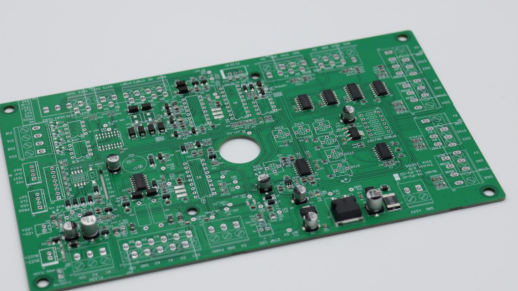
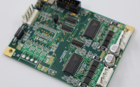
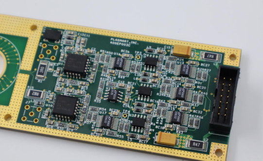
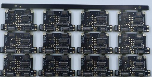
4. Classic Application Example: Post-SMT PCB Inspection
-
Target Defects: Solder paste defects, component presence/absence, correct value, placement accuracy, polarity, and solder joint quality.
-
Typical Flow:
-
The assembled PCB enters the AOI station.
-
Multi-angle lighting illuminates components and solder joints; the camera scans the entire board.
-
Software analyzes the images, comparing them to the board’s layout and component library.
-
Defects like misalignment, bridging, or missing chips are identified and classified.
-
The board is flagged, and data is sent to the repair station or MES (Manufacturing Execution System).
-
The essence of AOI is “to replicate human vision and surpass human judgment.” It combines precision opto-mechanical engineering for image capture with sophisticated image processing and artificial intelligence for decision-making. This enables 100% inline inspection, making AOI an indispensable pillar of smart factories and Industry 4.0. The integration of deep learning is transforming AOI from a simple defect detector into an intelligent process monitoring and predictive analytics tool.