The most common reflow soldering defects include solder bridging, tombstoning, cold solder joints, and voids, and they occur due to issues such as excess or misaligned solder paste, uneven heating, insufficient reflow temperature, and trapped gases during the solder melting and cooling process.
Solder bridging caused by excessive paste or misalignment
Solder bridging happens when too much solder paste or poor component alignment causes two adjacent pads to connect unintentionally.
In reflow soldering defects in PCB assembly, solder bridging is one of the most common issues. It occurs when molten solder flows beyond its intended pad and forms an unwanted electrical connection between two nearby pads.
This usually happens due to excess solder paste printing in SMT process or inaccurate stencil design. It can also occur if components are slightly misaligned during placement, especially in fine-pitch ICs.
For example, in smartphone PCB production, even a tiny excess of paste can cause a bridge between two IC pins, leading to short circuits and device failure.
Tombstoning effect in small passive components
Tombstoning happens when one side of a small component lifts up during reflow due to uneven heating or surface tension imbalance.
The tombstoning defect in reflow soldering is common in small components like resistors and capacitors. During heating, if one pad melts faster than the other, surface tension pulls the component upright like a “tombstone.”
This is usually caused by uneven heat distribution in PCB reflow process or inconsistent solder paste volume on each pad.
For example, in LED circuit boards or wearable devices, tiny 0402 components are highly sensitive to this defect because even small thermal differences can create imbalance.
Cold solder joints due to insufficient reflow temperature
Cold solder joints occur when solder does not fully melt, resulting in weak electrical and mechanical connections.
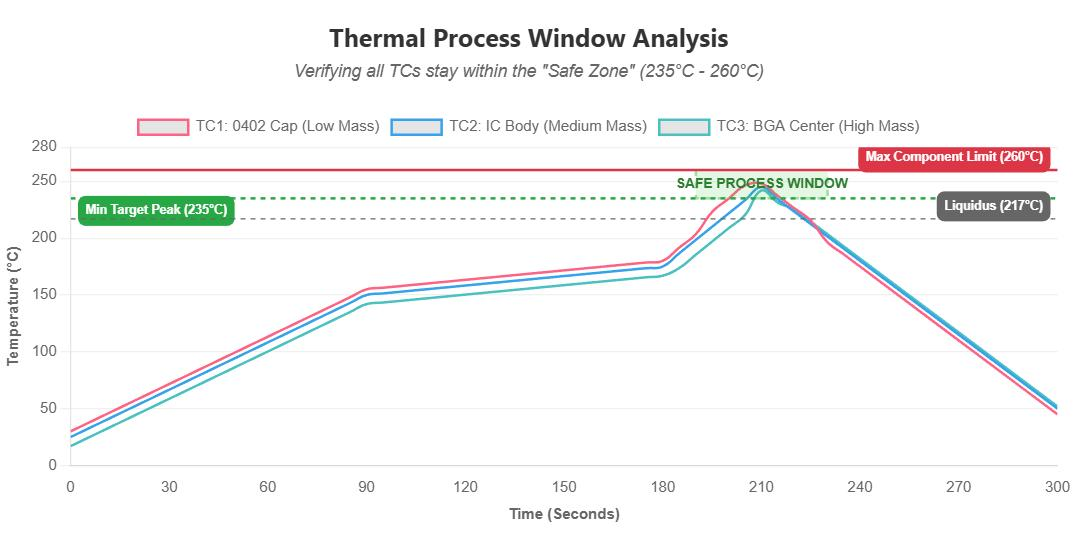
In cold solder joint defects in SMT reflow soldering, the solder paste does not reach the correct melting temperature or cooling is too fast before proper wetting occurs.
This creates dull, grainy-looking joints that may still look connected but have poor conductivity and low mechanical strength.
For example, in automotive control modules, cold joints can cause intermittent signal loss, especially under vibration or temperature changes.
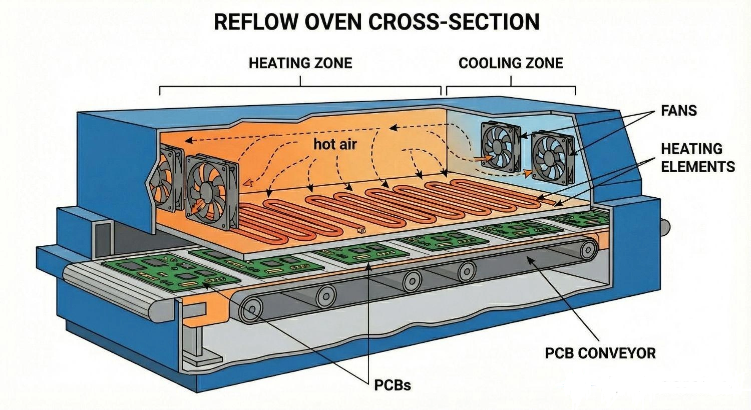
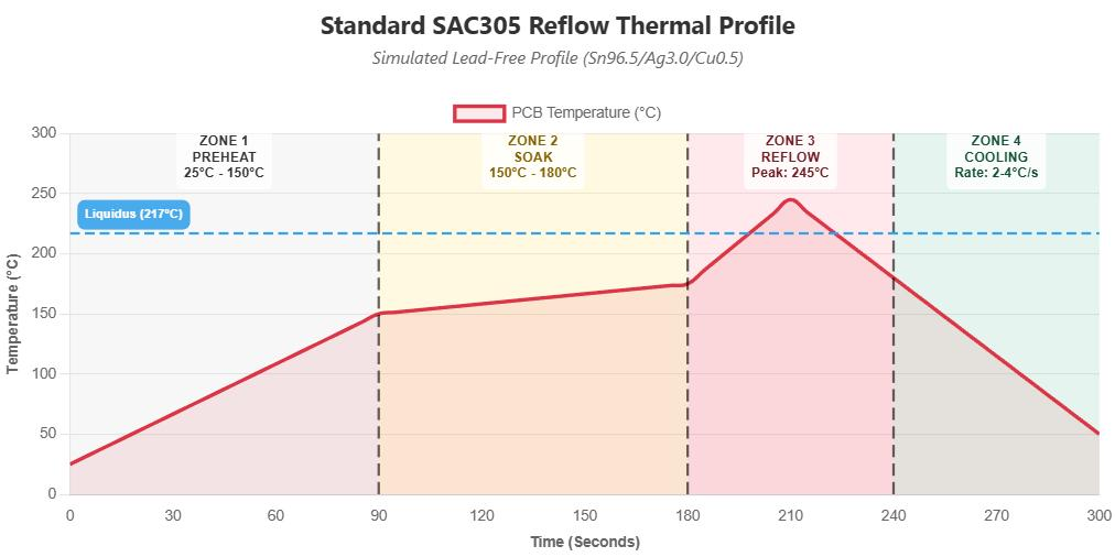
This defect is often linked to incorrect reflow oven temperature profile settings or insufficient peak temperature control.
Voids in solder joints and their impact on reliability
Voids are trapped gas pockets inside solder joints that reduce strength and heat conductivity.
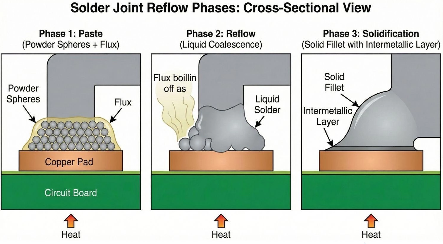
In reflow soldering void defects in PCB assembly, voids form when flux gases or air cannot escape during the melting stage. These gas pockets become trapped inside the solidified solder joint.
Voids reduce the effective contact area between solder and pad, which weakens both electrical and thermal performance. This is especially critical in high-power devices like LED modules or power electronics.
For example, in power IC packaging, excessive voiding can lead to overheating because heat cannot efficiently transfer through the solder joint.
Void formation is often controlled by optimizing reflow profile soak time, peak temperature, and vacuum-assisted reflow techniques in advanced manufacturing environments.