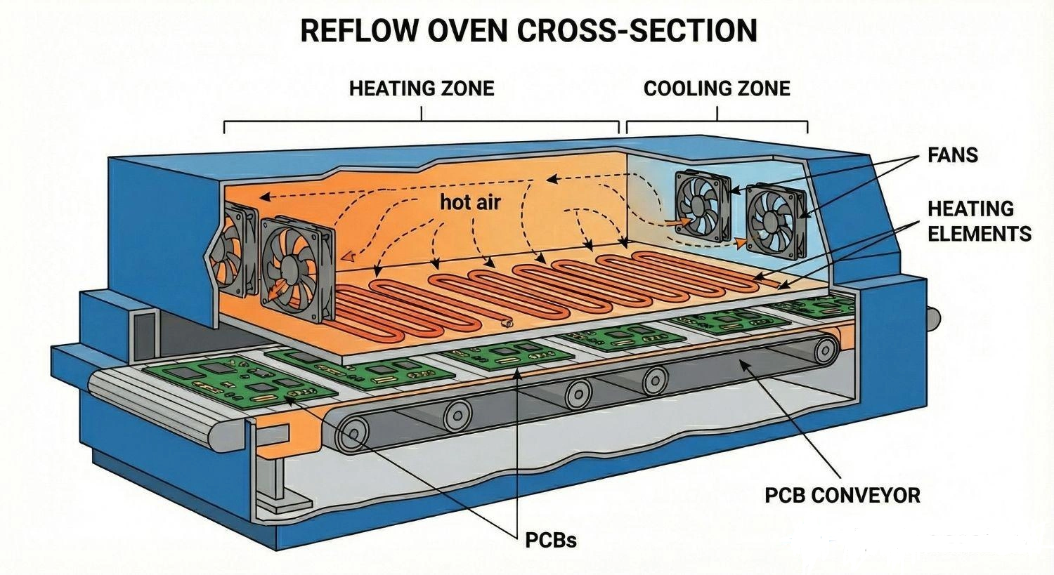
A reflow oven profile is a precisely controlled temperature curve used during PCB reflow soldering, and it affects soldering quality by determining whether solder joints form correctly—ensuring proper melting, wetting, and cooling to avoid defects like cold joints, overheating damage, and weak connections.
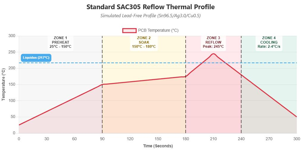
Key stages of a standard reflow temperature profile
A reflow oven profile is a controlled temperature curve that guides the PCB through heating and cooling stages to ensure proper solder melting and reliable joint formation.
A reflow soldering temperature profile in PCB manufacturing defines how temperature changes over time inside the reflow oven. It is not random heating—it is a carefully designed curve that ensures stable solder joints.
Ramp-up rate control (°C/sec)
The ramp-up stage gradually increases temperature, usually around 1–3°C per second, to avoid thermal shock. If heating is too fast, sensitive components like ceramic capacitors may crack. In real SMT production lines, engineers carefully tune this rate for different PCB thicknesses.
Soak time optimization
The soak zone holds the temperature steady so the entire PCB becomes uniform. This step is important in SMT reflow soldering profiles because thick and thin areas heat differently. Soak time also activates flux, which removes oxidation from copper pads.
Peak temperature window (lead-free vs. leaded solder)
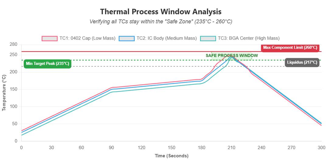
This is the highest temperature stage where solder melts. For lead-free reflow profiles, peak temperatures are typically 235°C–245°C, while leaded solder is lower, around 210°C–230°C. Staying within this window ensures proper wetting without damaging components.
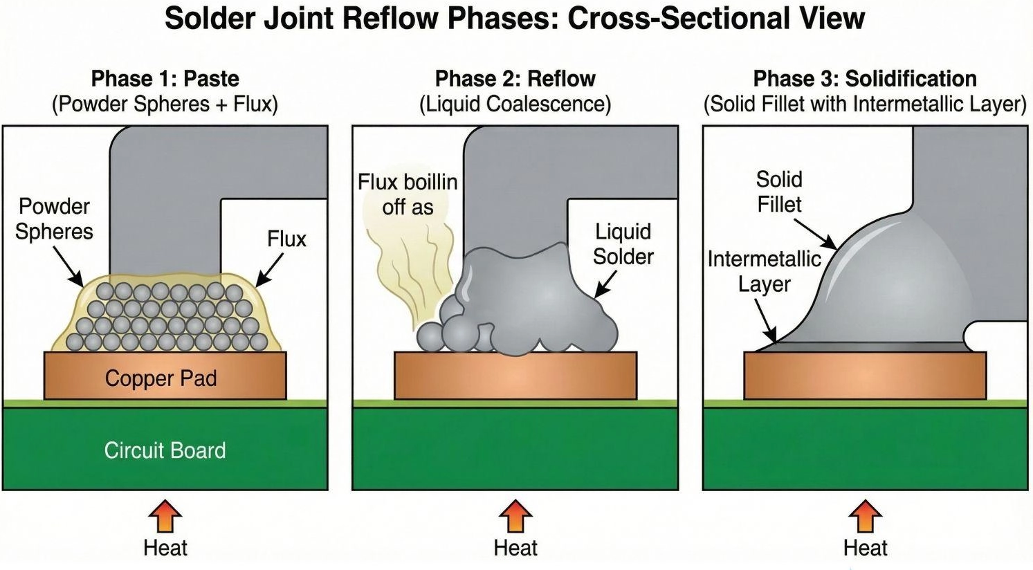
How temperature profiles impact solder joint reliability
Temperature profiles directly control whether solder joints are strong and defect-free or weak and unreliable.
Cold solder joints caused by insufficient heat
If the reflow oven temperature profile is too low, solder may not fully melt. This creates dull, weak joints called cold solder joints, which can cause intermittent failures in products like smartphones or automotive control boards.
Component damage caused by overheating
If temperature is too high or exposure time is too long, components can be damaged. For example, IC packages may delaminate or plastic housings may warp. This is a common issue in poorly calibrated PCB reflow soldering processes.
In practice, factories run test boards called “thermal profiling coupons” to ensure the oven settings match the product requirements before mass production.
Differences between lead-free and leaded reflow profiles
Lead-free and leaded solder require different temperature profiles because they melt at different temperatures and behave differently during reflow.
Higher melting point requirements for lead-free solder
Lead-free solder (commonly SAC alloys) melts at a higher temperature than traditional leaded solder. This means the lead-free reflow soldering profile must reach higher peak temperatures while still protecting components.
Adjustments in soak and peak zones
Lead-free profiles often require longer soak times and tighter control of the peak zone to ensure proper wetting. Leaded profiles are more forgiving and operate at lower thermal stress levels.