In the electronics manufacturing industry, Solder Paste Inspection (SPI) is a critical process for ensuring the quality of printed circuit board (PCB) assembly. Using sophisticated optical or laser technology, it comprehensively inspects the solder paste deposits on PCB pads before component placement and reflow soldering, thereby preventing soldering defects, improving production efficiency, and reducing manufacturing costs.
The Core Role of Solder Paste Inspection
Solder paste acts as a “bridge” connecting electronic components to the PCB, and its quality directly affects soldering reliability. Improper application of solder paste can lead to defects such as cold solder joints, bridging, and tombstoning, potentially causing product failure or safety hazards. Studies show that up to 70% of soldering problems originate in the solder paste printing process. SPI detects key parameters such as the volume, height, area, and alignment of the solder paste in real time, issuing early warnings when defects occur, preventing problems from flowing into subsequent processes, thus significantly reducing rework costs and material waste.
Inspection Technology and Equipment
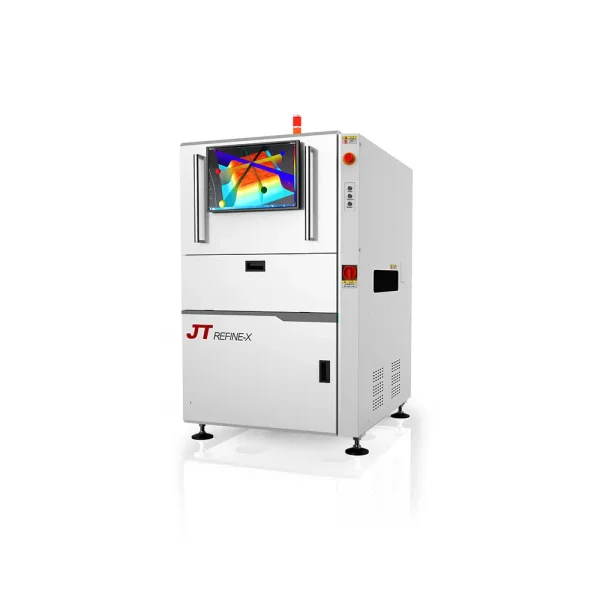
Modern SPI systems primarily employ 3D inspection technology, using laser triangulation or structured light projection to construct a three-dimensional model of the solder paste deposit. For example, the Vitrox V310i series equipment utilizes phase-shift measurement technology, coupled with a high-resolution camera, to achieve micron-level precision measurements at speeds up to 94 cm²/s. These devices can identify not only basic issues such as missing, excessive, or misaligned solder paste, but also analyze complex defects like board bending and bridging risks, providing data support for process optimization.
In contrast, traditional 2D SPI systems can only detect the coverage area and location of solder paste through planar images, with limited accuracy in measuring height and volume, and are gradually being replaced by 3D technology.
Inspection Process and Standards
SPI is typically deployed after solder paste printing and before component placement in an SMT production line. The inspection process includes:
1. Data Acquisition: A high-speed scanning head performs a full or partial scan of the PCB to acquire three-dimensional data of the solder paste.
2. Parameter Comparison: The measured data is compared with predefined standards (such as IPC-7525) to determine whether the solder paste volume, height, area, etc., are within acceptable ranges.
3. Defect Classification: The system automatically marks out-of-tolerance solder joints and classifies them into “Critical,” “Warning,” or “Acceptable” levels.
4. Feedback Adjustment: Detection results are fed back to the printing press in real time, automatically adjusting parameters such as stencil pressure and printing speed to achieve closed-loop control.
Application Scenarios and Benefits
SPI is widely used in consumer electronics, automotive electronics, and industrial control. For example, in smartphone motherboard production, BGA chips with a 0.3mm pitch require extremely high solder paste precision. SPI can detect height deviations at the 5-micron level, avoiding short-circuit risks. After introducing SPI, a certain automotive electronics manufacturer reduced the defect rate of cold solder joints in ECU modules from 3‰ to 0.2‰, reducing annual rework costs by millions of yuan.
From an economic perspective, the return on investment for SPI is significant. Taking a 500,000-point SMT line per month as an example, the introduction of SPI can reduce the reject rate of pick-and-place machines by 40%, reduce post-reflow soldering repair time by 65%, and reduce customer return costs by 80%. Furthermore, the process data accumulated through SPI can be used to analyze the impact of factors such as environmental humidity and stencil lifespan on solder paste printing, further optimizing production parameters.
Future Trends
As electronic products become increasingly miniaturized and high-density, SPI technology is evolving towards higher precision and greater intelligence. For example, the application of AI algorithms enables equipment to automatically learn optimal inspection parameters, reducing manual intervention; and its integration with AOI (Automated Optical Inspection) and X-ray equipment creates a quality traceability system covering the entire PCB assembly process. It is foreseeable that SPI will become one of the core tools for electronics manufacturing to move towards a “zero-defect” era.