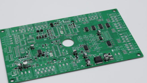
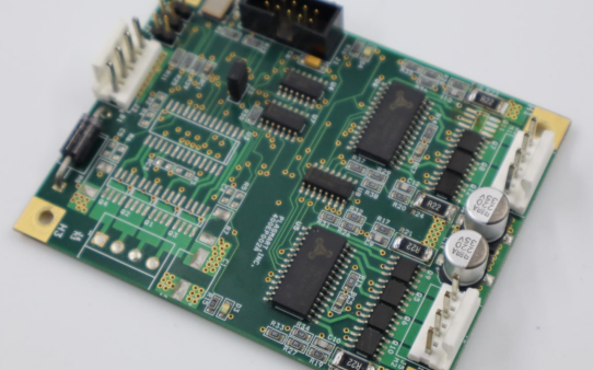
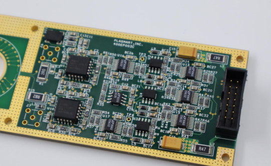
In the electronics manufacturing industry, solder paste printing is a core process in surface mount technology (SMT), and its quality directly affects the soldering reliability and product lifespan of circuit boards. However, traditional two-dimensional inspection technologies cannot capture the three-dimensional morphology of solder paste, making it difficult to meet the inspection needs of miniaturized, high-density electronic components. 3D solder paste inspection (3D SPI) technology has emerged to address this need, becoming a key tool for ensuring the quality of electronic manufacturing through high-precision three-dimensional measurement and intelligent analysis.
Technical Principles: Three-Dimensional Imaging and Precise Quantization
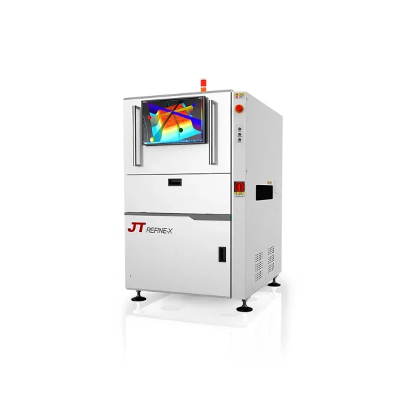
The core of 3D solder paste inspection lies in acquiring the three-dimensional morphological data of the solder paste. Mainstream technologies include laser triangulation, phase modulation profilometry (PMP), and structured light imaging. Taking the Vitrox V310i Optimus system as an example, it uses phase-shift measurement technology to generate a three-dimensional model of the solder paste through the phase changes of a white structured grating. This system is equipped with a 25MP high-resolution camera with an optical resolution of up to 4.5μm/px, enabling precise measurement of solder paste height, area, volume, and offset. Volume measurement accuracy reaches ±2%@6σ, and it can identify potential defects with thickness deviations exceeding 15μm.
Core Functions: Defect Prevention and Process Optimization
Located after solder paste printing and before component placement on the SMT production line, the 3D SPI system acts as a “quality gatekeeper.” Its core functions include:
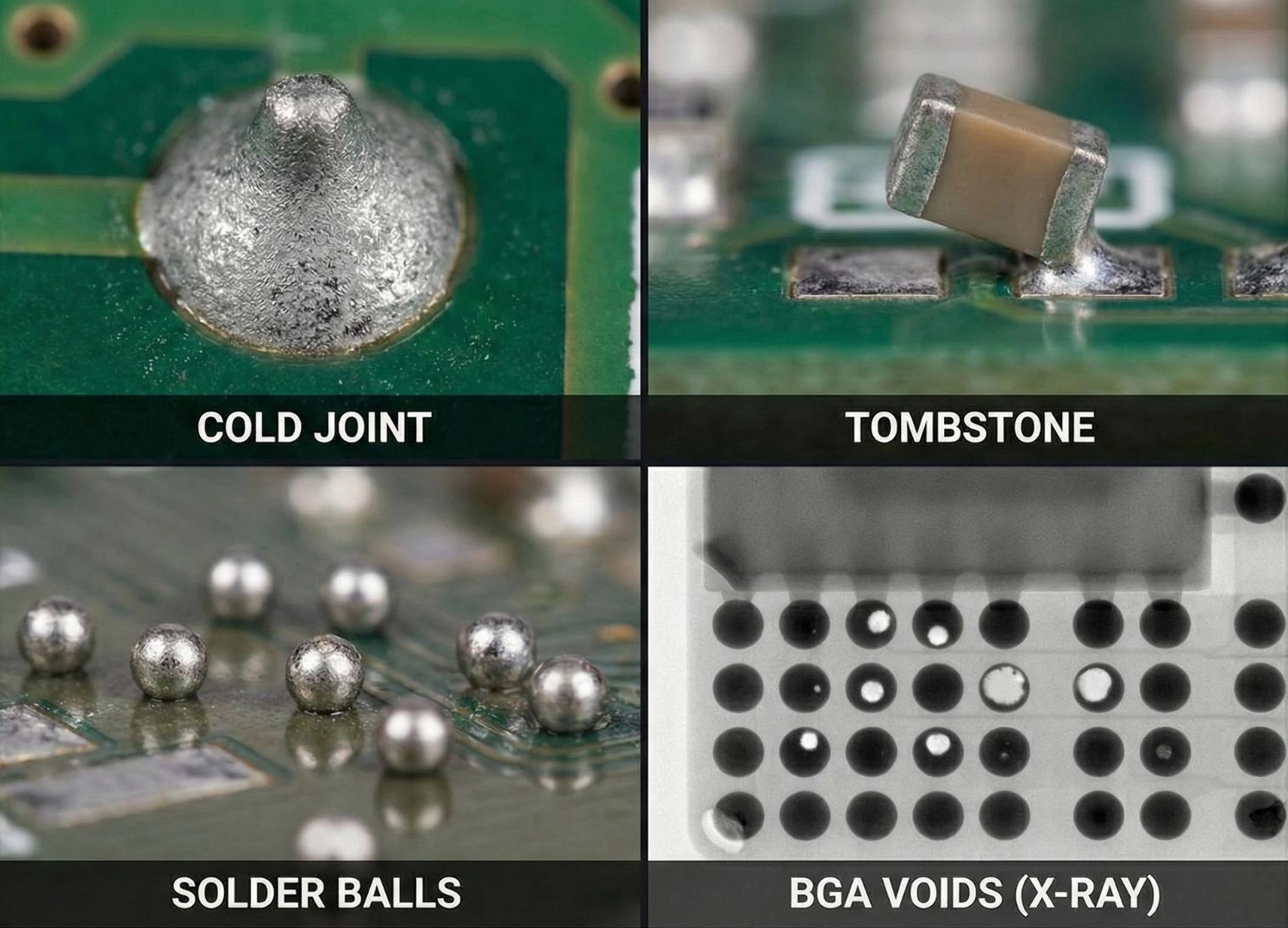
1. Defect Identification: Through three-dimensional quantitative analysis, it detects printing defects such as insufficient solder, excessive solder, collapsed edges, and bridging. For example, on the pads of 0201 components, the system can identify solder paste deposition with a volume deviation exceeding ±15%, preventing subsequent short circuits or cold solder joints.
2. Process Monitoring: It tracks key parameters such as solder paste height and area in real time, generating Statistical Process Control (SPC) charts. When parameters deviate from control limits, the system immediately alarms and feeds back to the printer, achieving closed-loop process adjustment.
3. Data Traceability: Integrating with Automated Optical Inspection (AOI) and X-ray Inspection (AXI) equipment, a complete defect propagation path map is constructed. For example, an automotive electronics manufacturer reduced its soldering defect rate from 3‰ to 0.2‰ by cross-referencing data from SPI and AXI.
Technological Advantages: A Balance of Accuracy, Speed, and Intelligence
Compared to traditional 2D inspection, 3D SPI offers significant advantages:
• Improved Accuracy: 3D imaging can capture micron-level height differences, avoiding misjudgments caused by solder paste color and PCB warpage in 2D inspection. For example, on flexible printed circuit boards (FPCBs), 3D SPI can accurately measure the solder paste thickness in locally recessed areas.
• Optimized Efficiency: High-speed inspection capabilities cover the demands of high-paced production lines. The V310i Optimus system achieves an inspection speed of 94 cm²/second, supporting 100% inspection without impacting production capacity.
• Intelligent Integration: AI algorithms and machine learning functions simplify operational processes. The system can automatically optimize inspection parameters, reducing manual intervention, and supports integration with MES systems to achieve real-time visualization of production data.
Application Scenarios: Quality Assurance Across Multiple Industries
3D SPI has been widely applied in consumer electronics, automotive electronics, and semiconductor packaging. For example:
• Smartphones: Inspecting the solder paste printing quality of BGA chips on the motherboard to prevent signal interference or system crashes.
• Automotive Electronics: Providing high-reliability testing for core modules of autonomous driving assistance systems, meeting automotive-grade lifespan requirements.
• Semiconductor Packaging: Inspecting solder bumps in system-in-package (SiP) systems to ensure the stability of electrical connections between chips and substrates.
Future Trends: Integration of Nanoscale Inspection and Industry 4.0
As electronic components evolve towards the nanoscale, 3D SPI technology is moving towards higher precision and greater intelligence. Future systems will integrate multispectral imaging and deep learning algorithms to achieve automatic defect classification and process risk prediction. Simultaneously, data interconnection under the Industry 4.0 framework will make SPI a core node in the intelligent manufacturing ecosystem, driving electronic manufacturing towards the goal of “zero defects.”