Understanding how solder paste inspection works is crucial to ensuring the quality and reliability of printed circuit boards (PCBs). Let’s review the inspection process and explore the key technologies that make it possible.

Inspection Process Overview
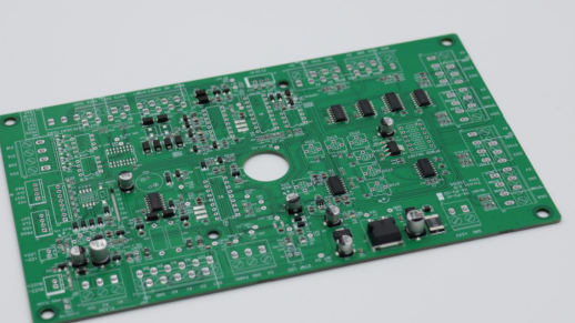
Solder paste inspection is a systematic process for evaluating the application of solder paste on a PCB. This evaluation ensures correct solder paste application, minimizes defects, and improves the overall quality of the finished product.
Key Technologies Used
Several key technologies combine to facilitate practical solder paste inspection:
- Cameras: High-resolution cameras capture detailed images of solder paste deposits. These images are critical for analyzing application quality and consistency.
- Sensors: Advanced sensors measure key parameters such as solder paste volume and height. This data is crucial for identifying defects.
- Lighting: Proper lighting enhances image clarity and helps the inspection system distinguish between different solder paste conditions. Techniques such as darkfield or brightfield lighting are often employed to optimize visibility.
Step-by-Step Explanation of the Solder Paste Inspection Workflow
Let’s break down the solder paste inspection workflow into three main steps:
1.PCB Preparation
Before applying solder paste, ensure the PCB is clean and free of contaminants. This preparation includes:
- Inspecting the circuit board for any debris or foreign objects.
- Ensuring the stencil used for applying the solder paste is correctly aligned.
A well-prepared PCB lays the foundation for accurate solder paste application.
2.Solder Paste Application
Solder paste is applied to the PCB using a stencil printing process or dispensing method. This step is crucial because the quality of the solder paste application directly affects the inspection results. Key factors to consider in this step include:
- Paste Consistency: The solder paste texture should be uniform to ensure proper flowability and adhesion.
- Application Technology: Correct technology helps achieve the required volume and shape for solder paste deposition.
3.Inspection: Once solder paste is applied, inspection is necessary. This involves the following:
- Image Capture: The inspection system uses a camera to capture images of the PCB with solder paste applied.
- Data Analysis: Advanced software analyzes the captured images, measuring key parameters such as the height, volume, and area of the solder paste deposit.
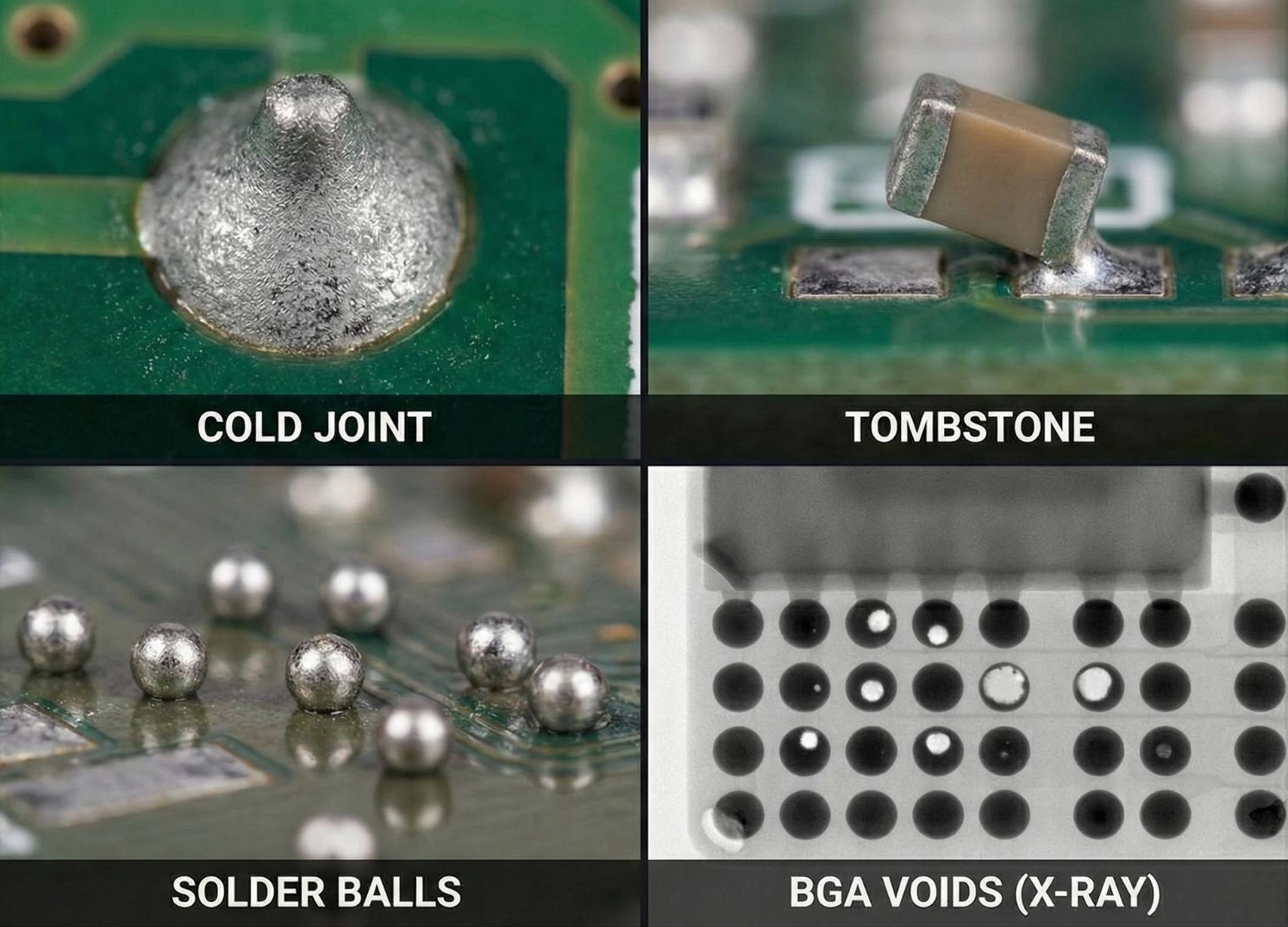
- Defect Detection: The system identifies any defects, such as insufficient or excessive solder paste, and generates a report for further review.
By following this structured workflow, manufacturers can ensure high-quality solder paste application, thereby reducing the likelihood of defects in the final product.