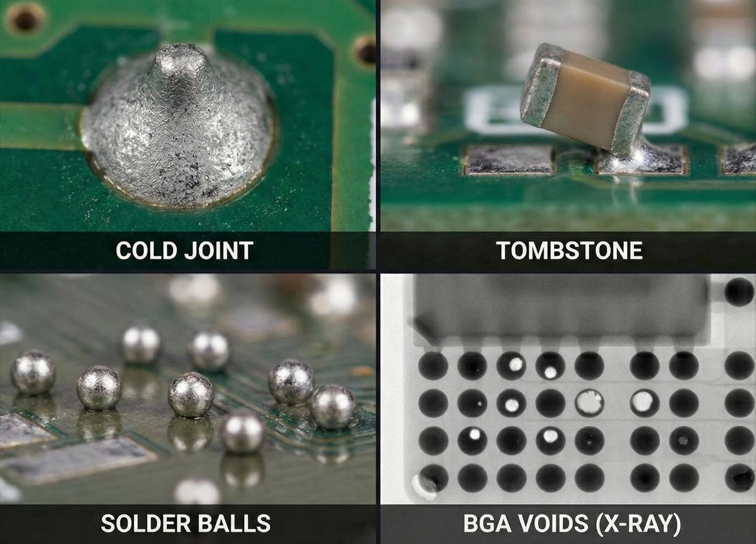
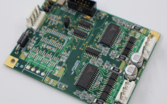
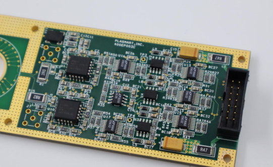
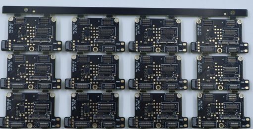
Even with advanced printing techniques, solder paste application can still go wrong. SPI is designed to detect these problems before they become bigger issues. Here are some common solder paste defects and how SPI helps identify them.

1. Insufficient Solder Paste
Insufficient solder paste on the pads can result in weak or incomplete solder joints. This is often caused by stencil clogging or uneven pressure during the printing process. SPI detects insufficient solder paste by measuring low volume (e.g., below 100 cubic micrometers) or reduced area coverage (e.g., less than 80%).
2. Excessive Solder Paste
Excessive solder paste can cause solder bridging or tombstoning, where components are lifted off the board during reflow. SPI identifies excessive paste by marking values for high volume (e.g., above 150 cubic micrometers) or height (e.g., above 180 micrometers) that exceed acceptable limits.
3. Solder Paste Bridging
Bridging typically occurs when solder paste connects two adjacent pads. This is usually caused by overprinting or misalignment. This defect can cause short circuits in the final product. The SPI system detects bridging by detecting solder paste deposits that cover or extend beyond the pad boundaries in abnormal areas.
4. Solder Paste Misalignment
If the solder paste is not centered on the pad, the component may not align correctly during placement. SPI captures misalignment by comparing the position of the paste to the center of the pad, marking offsets greater than 25 micrometers.
5. Uneven Solder Paste Distribution
Uneven distribution (solder paste being thicker in some areas than others) can lead to inconsistent soldering. 3D SPI technology maps the height and area of each deposit to identify variations that may affect quality.
Best Practices for Effective Solder Paste Inspection
To fully leverage SPI, manufacturers should follow these best practices:
Regularly calibrate equipment: Ensure SPI machines are calibrated to maintain the accuracy of measurements such as solder paste height and volume. Even a deviation of just 10 microns can affect results.
Use high-quality stencils: Well-designed stencils with clean apertures prevent issues such as insufficient paste or bridging. Regular cleaning after every 5-10 prints is recommended.
Set clear standards: Define acceptable ranges for solder paste volume (e.g., 100-150 cubic microns), height (e.g., 130-160 microns), and alignment (e.g., within 25 microns) based on your project requirements.
Monitor process trends: Use SPI data to track trends over time, such as recurring low-volume deposits, to identify and correct root causes such as stencil wear or printer settings.
Train operators: Equip your team with the skills to interpret SPI data and quickly adjust the printing process as defects are flagged.