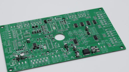
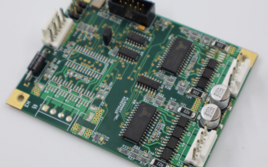
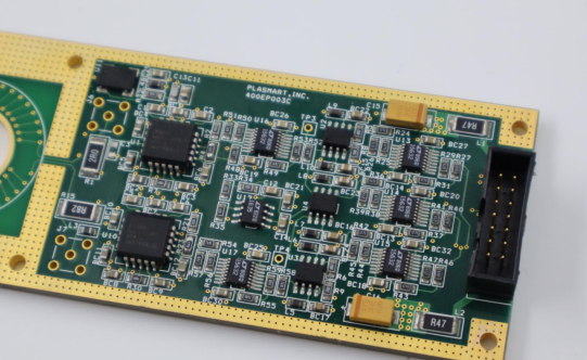
In the electronics manufacturing industry, with the rapid development of surface mount technology (SMT) towards miniaturization and high density, solder paste printing quality inspection has become increasingly important. 3D solder paste inspection technology, with its unique advantages, has become a key means of ensuring the quality of electronic products, demonstrating significant core competitiveness compared to traditional inspection technologies.
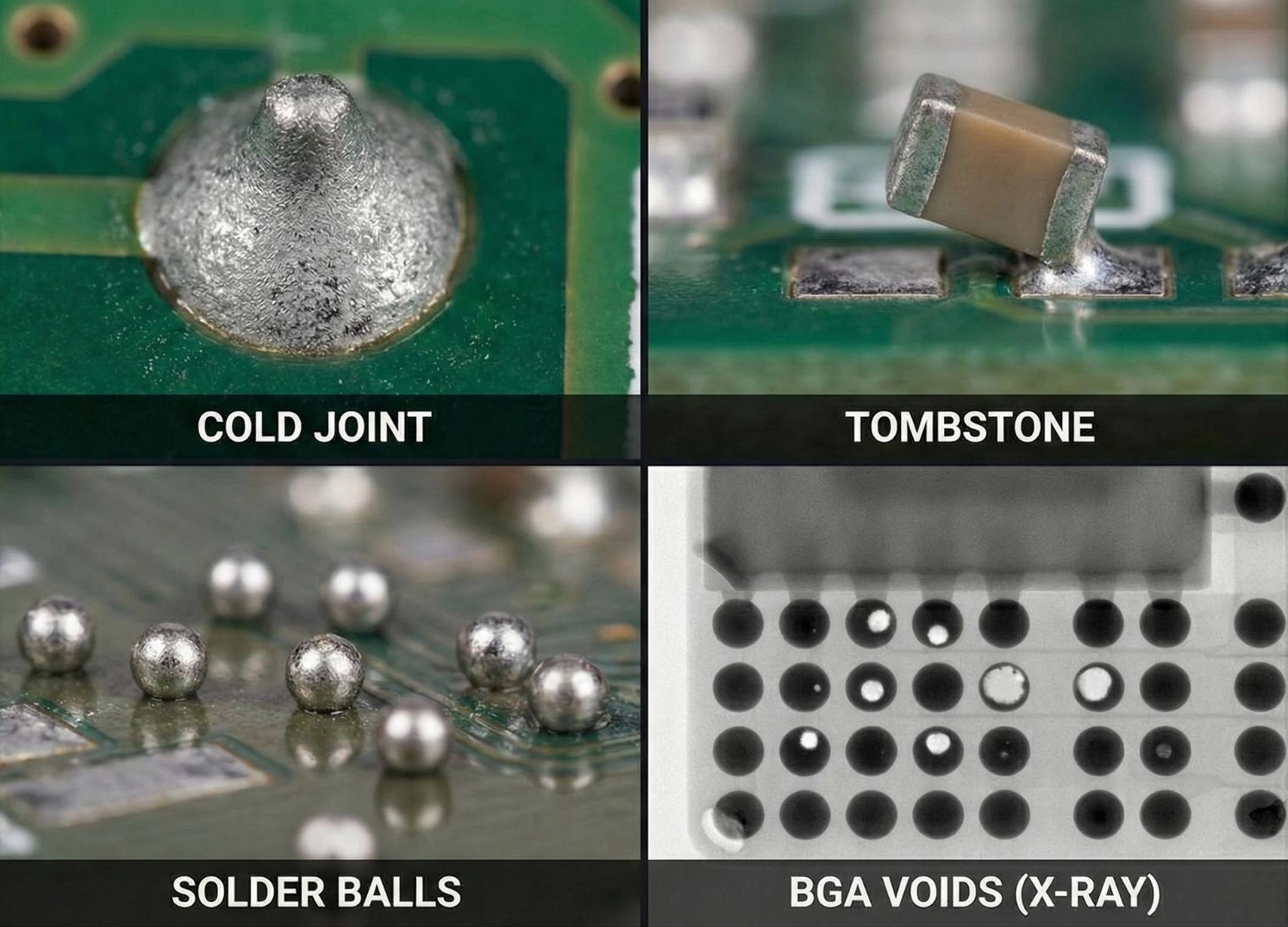
Precise quantitative analysis is the “killer app” of 3D solder paste inspection. Traditional 2D inspection can only obtain planar image information of the solder paste, and is powerless to measure key three-dimensional parameters such as solder paste volume and height. 3D inspection, using laser triangulation or structured light imaging technology, can construct a three-dimensional model of the solder paste, accurately measuring its height, area, volume, and other parameters. Taking high-precision 0201 components as an example, their pad sizes are extremely small, and even minute deviations in solder paste printing can lead to soldering defects. 3D inspection can accurately identify height fluctuations at the 5μm level, providing early warning of bridging risks and nipping potential quality problems in the bud, providing a solid guarantee for the manufacturing of high-precision electronic products.
Highly efficient defect identification capabilities significantly improve production efficiency. The 3D inspection system boasts high-speed scanning capabilities, enabling rapid and comprehensive inspection of all solder paste deposits on an entire PCB board. Inspection speeds reach tens of square centimeters per second, fully meeting the demands of large-scale production lines and achieving 100% inspection without impacting overall capacity. Simultaneously, its powerful algorithms can quickly classify detected defects, such as insufficient solder, excessive solder, and collapsed edges, providing detailed defect location and type information. This facilitates timely problem identification and resolution by operators, reducing production downtime and improving overall production line efficiency.
Intelligent process optimization is another highlight of 3D inspection. It not only detects defects but also provides optimization suggestions for production processes through the analysis of large amounts of inspection data. For example, when a region is found to have generally low solder paste height, the system can provide feedback, prompting adjustments to the printing press pressure, speed, or stencil parameters, thereby achieving closed-loop process control. This data-driven intelligent optimization method helps continuously improve solder paste printing quality, reduce defect rates, and enhance product consistency and reliability.
Furthermore, 3D solder paste inspection also possesses excellent compatibility and scalability. It can seamlessly integrate with other inspection equipment such as Automated Optical Inspection (AOI) and X-ray Inspection (AXI) to form a complete electronic assembly quality inspection system, providing comprehensive quality monitoring solutions for electronic manufacturing enterprises.
3D solder paste inspection, with its precise quantitative analysis, efficient defect identification, intelligent process optimization, and excellent compatibility, has become an indispensable technology in the electronic manufacturing field. It helps companies improve product quality, reduce production costs, enhance market competitiveness, and drive the electronic manufacturing industry to a higher level of development.