In the electronics manufacturing field, 3D solder paste inspection technology, with its unique advantages, is becoming a key force in ensuring product quality and driving industrial upgrading. As electronic components rapidly evolve towards miniaturization and high density, 3D solder paste inspection technology is ushering in unprecedented development opportunities, with broad prospects and great potential.
Technological Upgrades Drive Dual Improvement in Accuracy and Efficiency
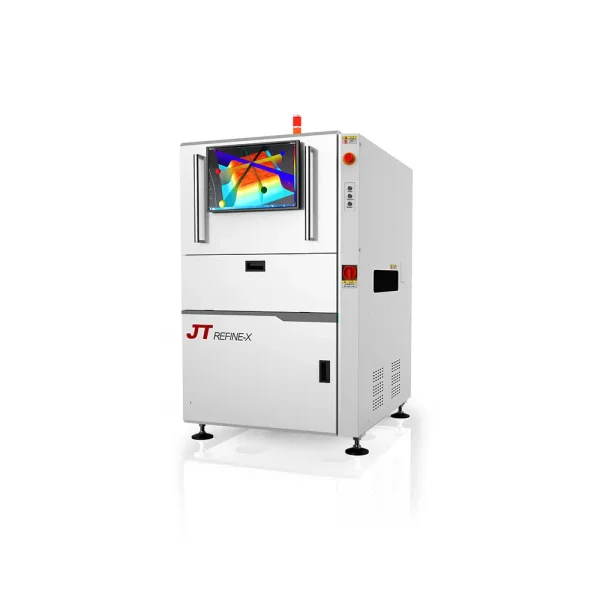
Currently, 3D solder paste inspection technology has achieved a leap from the micrometer level to the nanometer level. Taking the Vitrox V310i series equipment as an example, it adopts phase-shift measurement technology, combined with a 25MP high-resolution camera, achieving a detection resolution of 0.37 micrometers. Some high-end products can even achieve micrometer-level detection capabilities of ±0.8 micrometers. This improvement in accuracy allows the equipment to accurately capture minute defects in the solder paste printing process, such as height fluctuations at the 5-micrometer level, providing a solid guarantee for the manufacturing of high-precision electronic products. At the same time, the inspection speed is also constantly improving. Mainstream equipment can achieve inspection speeds of tens of square centimeters per second, meeting the rhythm requirements of large-scale production lines and achieving 100% inspection without affecting overall production capacity.
Intelligent Transformation Empowers End-to-End Quality Control
The integration of artificial intelligence and machine learning technologies is driving 3D solder paste inspection towards intelligentization. Through deep learning algorithms, the equipment can automatically identify complex defect types, such as bridging and cold solder joints, and perform precise classification, significantly improving defect identification accuracy. More importantly, the intelligent system can also predict potential process risks based on historical data and adjust printing parameters in advance, achieving a shift from “defect detection” to “defect prevention.” Furthermore, the deep integration of 3D inspection equipment with the MES system of SMT production lines constructs a closed-loop control system of “inspection-data feedback-process optimization,” helping companies improve overall production efficiency and reduce rework costs.
Expanding Application Scenarios Creates New Growth Points
The application scenarios of 3D solder paste inspection technology are extending from traditional consumer electronics to high-end fields such as automotive electronics and semiconductor packaging. In the automotive electronics field, the stringent reliability requirements of automotive-grade chips are driving the upgrade of 3D inspection equipment towards “all-scenario adaptability,” enabling it to withstand harsh environments such as extreme temperatures and vibrations to ensure soldering quality. In the semiconductor packaging field, the widespread adoption of advanced packaging technologies such as Chiplet has placed higher demands on the precision and consistency of solder paste printing, making 3D inspection equipment a key tool for ensuring packaging yield. Furthermore, with the rise of emerging technologies such as MiniLED and flexible circuit boards, 3D solder paste inspection technology will find applications in more niche areas, bringing new growth points to the industry.
Domestic Substitution Accelerates the Rise of Local Enterprises
In international market competition, local enterprises are rapidly rising thanks to technological breakthroughs and cost advantages. Domestic manufacturers, represented by Aopu Optoelectronics and Juzi Technology, have achieved internationally advanced levels in inspection precision, speed, and intelligence through independent research and development of core technologies. They are also seizing market share in the low-to-mid-range market with more competitive prices and gradually penetrating the high-end market. With increased policy support and coordinated development of the industrial chain, domestically produced 3D solder paste inspection equipment is expected to achieve breakthroughs in more niche areas, continuously promoting the import substitution process in the industry.