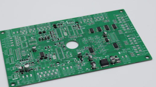
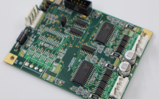
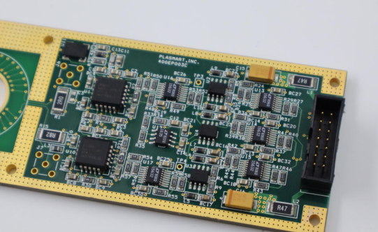
In the electronics manufacturing industry, solder paste printing quality is a core factor determining product reliability. Traditional solder paste inspection (2D SPI) and 3D solder paste inspection (3D SPI), as two key technologies, are reshaping the quality control system of SMT (Surface Mount Technology) through different inspection dimensions. This article will analyze the essential differences between the two from three dimensions: technical principles, inspection accuracy, and application scenarios.
Technical Principles: From 2D Projection to 3D Modeling
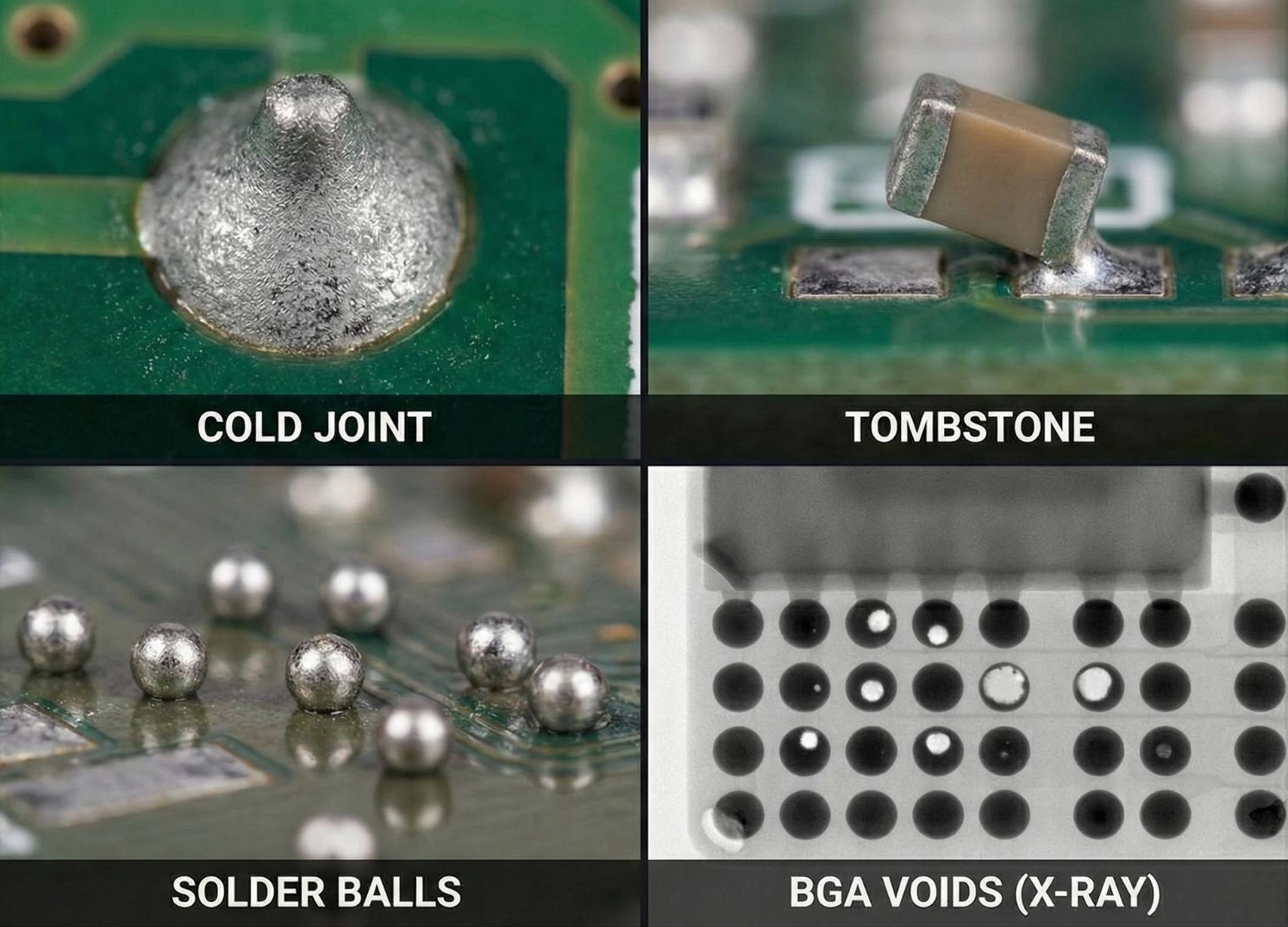
Traditional 2D solder paste inspection relies on optical cameras to capture 2D images of the solder paste. By comparing the pad contours with the solder paste coverage area, defects such as insufficient solder and bridging are identified. Its essence is 2D projection analysis, which cannot capture the vertical dimension information of the solder paste. For example, when the solder paste has a “central depression” due to stencil wear, 2D inspection may miss it because the overall coverage area meets the standard, but the actual height deviation has exceeded the process tolerance range.
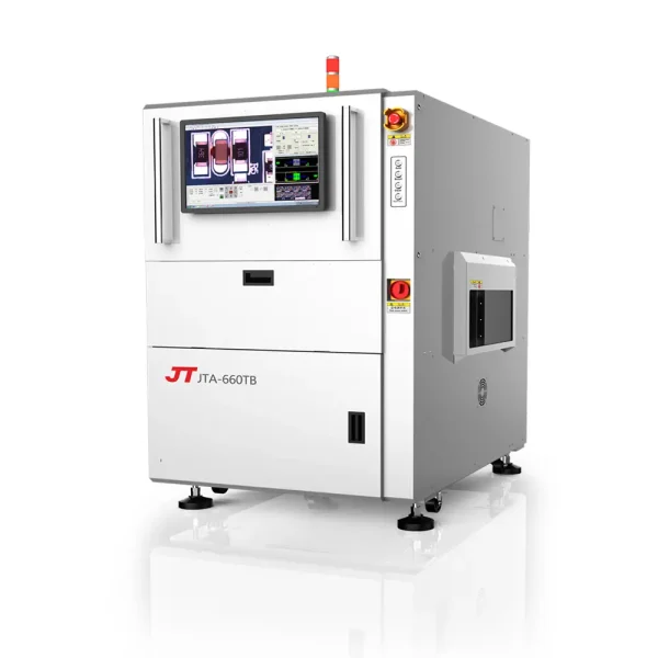
3D solder paste inspection, on the other hand, uses laser triangulation or structured light imaging technology to construct a 3D morphological model of the solder paste. Taking the Vitrox V310i series as an example, it employs Phase Shift Measurement (PSP) technology, coupled with a 25MP high-resolution camera, to achieve an optical resolution of 4.5μm/px, accurately measuring the height, area, volume, and shape of solder paste. This 3D modeling capability allows 3D inspection to identify defects that 2D technology cannot capture, such as solder paste spikes, collapsed edges, and localized thickness unevenness.
Inspection Accuracy: A Leap from Micrometers to Nanometers
The accuracy of 2D inspection is limited by optical resolution and focusing method. Manually focused 2D equipment has significant human error; even autofocus models often have volume measurement errors exceeding ±5%. For example, on the pads of a 0201 component (0.6mm × 0.3mm), 2D inspection may not be able to distinguish a height difference of 10μm, a deviation sufficient to cause a short circuit after reflow soldering.
3D inspection, through non-contact laser scanning, improves volume measurement accuracy to ±2%@6σ (an industry benchmark). Taking BGA chips on a smartphone motherboard as an example, with a pad spacing of only 0.3mm, 3D inspection can identify height fluctuations at the 5μm level, providing early warning of bridging risks. Furthermore, 3D technology can also predict post-reflow misalignment risks through morphological analysis—when the solder paste height standard deviation exceeds 15μm, the system will warn of an increased component displacement probability, providing data support for process optimization.
Application Scenarios: From General Inspection to High-End Manufacturing
2D inspection, due to its lower cost, is still widely used in scenarios with lower precision requirements, such as PCB assembly in industries like home appliances and lighting. However, its limitations are becoming increasingly apparent with the trend of miniaturization: when component sizes shrink to 0.1005 (0.4mm × 0.2mm), the false negative rate of 2D inspection may exceed 30%, failing to meet the high reliability requirements of fields such as automotive electronics and medical equipment.
3D inspection, on the other hand, has become a standard feature in high-end manufacturing. In the automotive electronics field, its early defect prevention capabilities can reduce rework costs by more than 10 times. In the semiconductor packaging field, 3D inspection can accurately measure micron-level defects in solder bumps and substrate lead frames, supporting yield improvements in advanced packaging (such as SiP and Flip Chip). For example, after introducing 3D inspection, a communications equipment manufacturer reduced the rate of cold solder joints on its 5G base station PCBs from 0.5% to 0.02%, saving tens of millions of yuan in annual rework costs.
Technological Evolution: From Single Inspection to Intelligent Closed-Loop
Modern 3D inspection equipment has transcended the traditional scope of quality inspection, evolving into an “intelligent process consultant.” Taking the Vitrox V310i as an example, its integrated AI programming function can automatically recognize Gerber files and generate inspection programs, reducing manual setup time by 90%. Through linkage with the MES system, 3D inspection data can be fed back to the printing press in real time, automatically adjusting parameters such as stencil pressure and printing speed, constructing a closed-loop control system of “inspection-analysis-optimization.” This intelligent transformation upgrades 3D inspection from a quality control tool to a production efficiency engine.
The evolution of solder paste inspection technology from 2D to 3D is essentially a microcosm of the pursuit of “zero defects” in electronic manufacturing. As component dimensions approach physical limits and market demands for reliability become increasingly stringent, 3D inspection, with its three-dimensional, precise, and intelligent characteristics, is becoming the lifeline of quality in high-end electronic manufacturing.