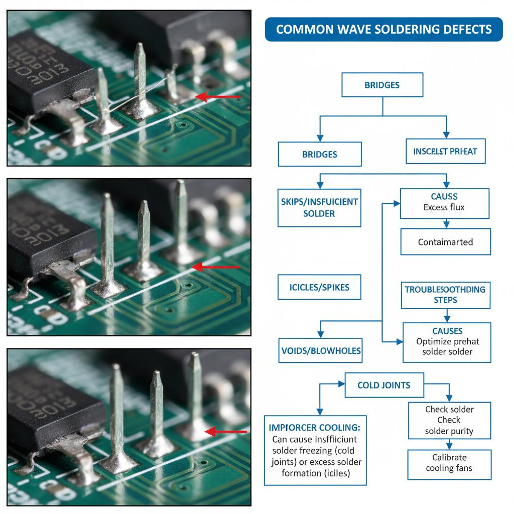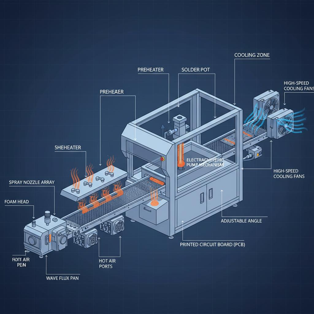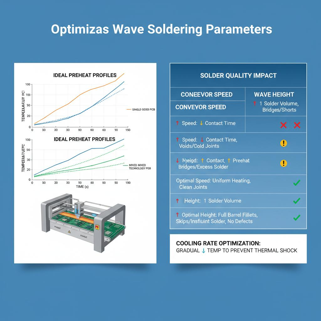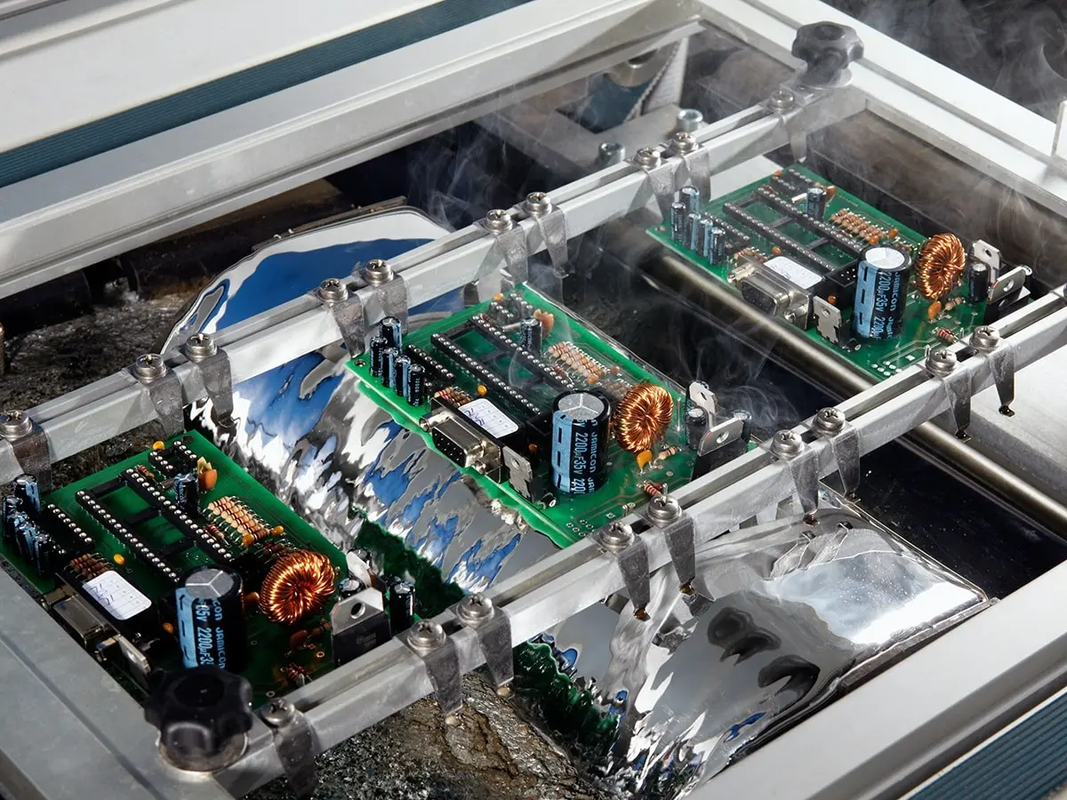

When circuit boards first appeared, they used traditional through-hole components (OSB) designs. Almost all boards at that time required wave soldering, and initially, boards were only single-sided.
Later, with the invention of surface mount technology (SMD), a hybrid approach combining SMT (Surface Mount Technology) and wave soldering began. However, a large number of components could not be converted to SMD processes, requiring a mix of traditional OSB and SMD components. After SMT assembly, the board still needed to undergo manual OSB assembly before wave soldering. Because of these process requirements, the board design had to arrange all OSB components on one side, while the other side was used for wave soldering. The SMD components on the wave soldering side had to be secured with glue to prevent them from falling into the solder bath during wave soldering.
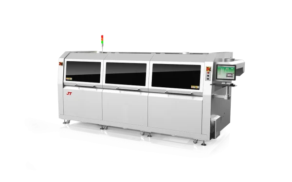
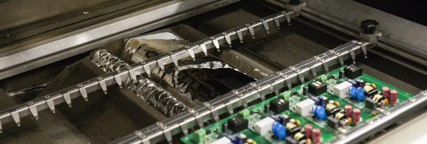
Because wave soldering involves a board immersed in molten solder, there are many limitations in PCB design and manufacturing. Additionally, some components cannot be placed on the solder bath surface.
To achieve better wave soldering quality, here are some design guidelines for component placement in the wave soldering process. It is recommended that PCB layout engineers collaborate with the factory’s process engineers before designing the PCB to determine the wave soldering direction and place components according to the wave soldering design guidelines. Below, I’ve summarized some wave soldering rules I know:
1. For areas that will be wave soldered, vias should ideally be plugged to prevent solder overflow onto the component surface during wave soldering, causing unpredictable short circuits.
2. For connector components, the straight lines of the connector pins should be parallel to the wave soldering direction. This prevents short circuits between pins and allows for better solder adhesion.
3. If small components such as resistors, capacitors, and inductors from SMT assembly need to be wave soldered, the components should be perpendicular to the wave soldering direction.
4. If there is a SOIC (Sort of ICs with solder pads on both sides of the component), its entire row of solder pads should be parallel to the direction of wave soldering.
5. Please note that only single-row or double-row solder pad components are suitable for wave soldering. Components with four-sided solder pads are not recommended for wave soldering. Although some people have tried to wave solder four-sided solder pad ICs at a 45-degree angle, this is very likely to cause short circuits.
6. To avoid the shadow effect, taller and larger components should be positioned behind the wave soldering direction.
7. Components containing 0402 and smaller are not recommended for wave soldering, as they will cause short circuits. In fact, 0603 size is almost the limit.
Suggested Hand Insertion Order for Wave Soldering (These rules were originally designed for boards with 10 or more hand inserts, but I believe they should also apply to some selective wave soldering boards):
1. Insert tightly fitted components first, such as connectors with bent leads (kinks) for external communication. This prevents vibrations from dislodging other pre-inserted components when inserting tight parts.
2. When inserting components, the right hand should insert from the upper left to the lower right; the left hand should insert from the upper right to the lower left to avoid components obstructing hand movements.
3. Insert lower-profile components first, then higher-profile components, to avoid taller components hindering hand movement. (For example, the resistor between two connectors.)
4. Ideally, identical components should be inserted at the same station. (This reduces the chance of incorrect insertion and component misplacement.)
5. Components inserted by the same operator should ideally be grouped together in one area, allowing the operator to focus on the same area and reducing the risk of errors.
6. Components with the same appearance but different part numbers should be avoided at the same workstation to prevent confusion.
7. Polarized parts should be avoided in the same workstation whenever possible. Otherwise, the workstation will be overloaded.
8. Each workstation should strive to have the same working hours.