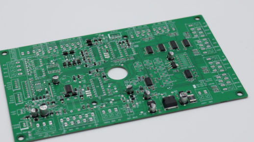
The Impact of Solder Joint Microstructure on Reliability
The internal microstructure of solder joints, as well as the intermetallic compound (IMC) structure at the solder-PCB substrate interface, determines the mechanical properties of the solder joint. Soldering processes, subsequent solid-phase aging, and thermal cycling further influence the initial microstructure and its evolution. An ideal IMC structure should form at the interface to achieve good wettability and metallurgical interconnection, resulting in satisfactory solder joint strength and reliability. The internal microstructure of the solder joint reveals the microscopic properties of the material, and existing microscopy and techniques can be used to obtain this information.
• Lead Solder Joints
In tin-lead alloys, the microstructure consists of tin-rich and lead-rich phases.
• Lead-Free Solder Joints
In SAC alloys, the metallurgical reaction between Sn and minor elements such as Ag and Cu is the main factor determining its application temperature, solidification mechanism, and mechanical properties.
According to the binary phase diagram, there are three types of binary eutectic reactions among the three elements mentioned above:
a) Ag and Sn react at 221°C to form a eutectic structure with Sn as the base phase and an ε-IMC (Ag₃Sn) phase.
b) Cu and Sn react at 227°C to form a eutectic structure with Sn as the base phase and an η-IMC (Cu₆Sn₅) phase.
c) Ag and Cu also react at 779°C to form a eutectic alloy composed of Ag-rich α phase and Cu-rich α phase.
Material composition determines the microstructure, which in turn determines the failure mode. During product application, microstructure promotes the formation of microparticles. Particle dispersion, uniform distribution, and granulation are beneficial for improving fatigue resistance. However, fatigue life decreases when acidification, brittle phases, excessive voids, and stress concentration occur. Controlling the microstructure to ensure uniform distribution of plastic deformation within a small area is an effective measure to improve fatigue strength.
The Influence of IMC Microstructure on Reliability at Solder Joint Interfaces
• Microstructure of Intermetallic Compounds at the Interface
a) Shape and Pattern
The η-Cu<sub>6</sub>Sn<sub>5</sub> layer has three shapes and structures:
1) Rough honeycomb layer. This layer contains dendritic crystals in its cross-section, with large intercrystalline spaces, forming a rough interface in contact with the solder. The structure is not dense.
2) Dense layer on a corrugated interface. This layer is similar in shape to the dendritic crystal particles, but has a denser chemical composition. The interface in contact with the solder is corrugated.
3) Dense layer on a flat interface. With increasing lead content, temperature, and reaction time, the shape and structure of the η layer begin to change from a rough honeycomb layer to a dense layer on a corrugated interface.
b) Influencing Factors
1) Higher cooling rates lead to the formation of a flat η phase layer, while lower cooling rates lead to the formation of a small, tumor-like η phase layer. 2) Shorter reflow times result in the formation of a flat η-phase layer, while longer reflow times result in the formation of small, tumor-like or scallop-like η-phase layers.
c) Peeling
The intermetallic compound (IMC) initially formed between the pad and the liquid solder can sometimes separate from the interface as the reflow time increases. This phenomenon is often associated with nickel. For example, it is more likely to occur on ENIG nickel platings. 1) At the interface of ENIG nickel platings with different phosphorus contents, IMC peeling occurs. The degree of peeling depends on the increase in phosphorus content and the extension of reflow time. 2) Some lead-free solders (Sn3.5Ag, Sn3.5Ag3.0Bi, and SAC387) and certain types of plating substrates [Cu, Ni(P)/Au, and Ni(P)Pd/Au], after reflow soldering at temperatures below 250°C for 20 minutes, exhibit intermetallic compounds (IMCs) at the interface, as well as most of the IMC layer formed by the first two solders, which may deflect or peel off from the interface, leaving only a thin layer of IMC on the interface. For SAC387 solder on [Ni(P)/Au and Ni(P)/Pd/Au] substrates, the (Cu,Ni)6Sn5 intermetallic compound (IMC) can bond well with the interface. However, for nickel-plated substrates, all three lead-free solders can bond well with the Ni3Su4 intermetallic compound (IMC).
d) Effect of Au on the intermetallic compound between SAC solder and the copper substrate
The intermetallic compound (IMC) formed by copper and SAC solder is granular. Adding 0.1 to 5 wt% gold to SAC387 resulted in a eutectic phase at 204.5 °C containing four compounds (AuSn<sub>4</sub>, Au<sub>3</sub>Sn, β-Sn, and Cu<sub>6</sub>Sn<sub>5</sub>). With the formation of the Au-Cu-Sn ternary metal compound, most of the gold in the solder migrates outwards and moves towards the interface. During the interfacial reaction, the gold distribution morphology changes from a typical scalloped pattern to a compound-like structure composed of (Au, Cu)<sub>6</sub>Sn<sub>5</sub> crystal grains and uniformly distributed island-like β-Sn.
• Growth of the Interfacial IMC Layer
The growth of the interfacial intermetallic compound (IMC) layer has a significant impact on solder joint reliability. Studies show that there is no stable relationship between IMC thickness and time. Liquid-phase condensation inhibits IMC growth, leading to uneven growth.
For lead-plated components, IMC growth exhibits a roughly linear relationship with the square root of time, consistent with dispersion patterns. However, for tin-lead-plated components, the IMC growth of SAC solder shows a distinct trend.
• Elemental Distribution at the Solder Joint Interface
Based on high and low temperature impact tests and high temperature tests, it can be observed that the Ag₃Sn network structure slightly decreases during the high-temperature test and clearly transforms into a granular Ag₃Sn phase, but the solder strength remains unaffected. The high-temperature test is used to accelerate the growth of the interface alloy layer. For lead-plated components, the alloy growth amount exhibits a roughly linear relationship with the square root of time. The growth process is carried out under a certain dispersion control rate. Nevertheless, the formed compound still significantly reduces the strength of the solder joint in both high and low temperature impact tests and high-temperature tests.
Lead-free solder joints have higher hardness and strength and less deformation than tin-lead solder joints, but this does not necessarily mean that lead-free solder joints have high reliability. Due to the poor wettability of lead-free solder, defects such as voids, displacement, and post-stakes are more likely to occur, and the void size is often larger.
• Brittleness and its Mechanism
1) A prolonged reaction between the nickel (P) plating layer and the tin-lead solder can create Kirkendal voids around the nickel surface. The brittleness issue becomes more complex when the solder contains copper. The ternary metal compound (Cu, Ni)<sub>6</sub>Sn<sub>5</sub> accumulates on the Ni<sub>3</sub>Sn<sub>4</sub> layer formed on the nickel surface, creating voids at the Ni<sub>3</sub>Sn<sub>4</sub>/(Cu, Ni)<sub>6</sub>Sn<sub>5</sub> interface during aging. Similar problems occur when using SAC solder to join nickel, as this solder alloy contains a copper source.
2) Black pads are a unique phenomenon closely related to brittleness, especially common in ENIG nickel/gold pads. Due to insufficient solderability of the Ni(P) surface, significant brittleness occurs in or around the pad, ultimately leading to reduced mechanical fatigue strength. Black pads are closely associated with solder joint cracking. Furthermore, the detrimental black pad effect is also related to another type of brittleness: the degradation of the optimal metal alloy structure over time.
3) On ENIG nickel/gold pads, SAC solder plays a more significant role than SnPb solder when the IMC structure undergoes black pad effect and aging due to brittleness. Lead-free soldering should avoid or minimize brittle changes caused by the thickening of the gold layer in the nickel/gold coating.
4) Even with the most common thermal cycling, solder joints are typically required to withstand the creep loads generated in each thermal cycle. Therefore, the intermetallic compound (IMC) structure on the pads must be able to withstand the loads from solder creep. External mechanical loads, especially those caused by system mechanical shocks, can lead to very severe solder creep because the deformation caused by creep to the solder joint is excessive. Therefore, even if the IMC structure can fully withstand thermal cycling, the weakest connections will emerge in shear or tensile force tests.
5) Au in SnPb-containing solder added during reflow soldering gradually returns to the Ni surface during subsequent aging, causing (Ni, Au)₃Sn₄ to accumulate on the Ni₃Sn₄ intermetallic compound. The resulting interface is unstable and decreases with increasing (Ni, Au)₃Sn₄ thickness.
The Harm of Solid-State Aging to Solder Joint Reliability
Solid-state aging can lead to thickening of the intermetallic compound (IMC), changing its shape from a corrugated to a flat, uniform layered structure. During solid-state aging, excessive intermetallic IMC is generated, accompanied by the segregation of some chemical elements that do not participate in the IMC formation process. Because the Kirkendall effect leads to a decrease in material density during IMC formation, excessive solid-state aging will create excessive cavities at the pad/solder interface.