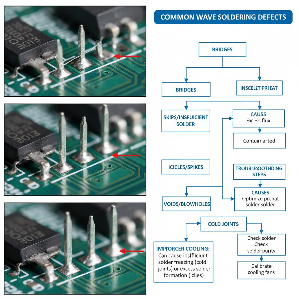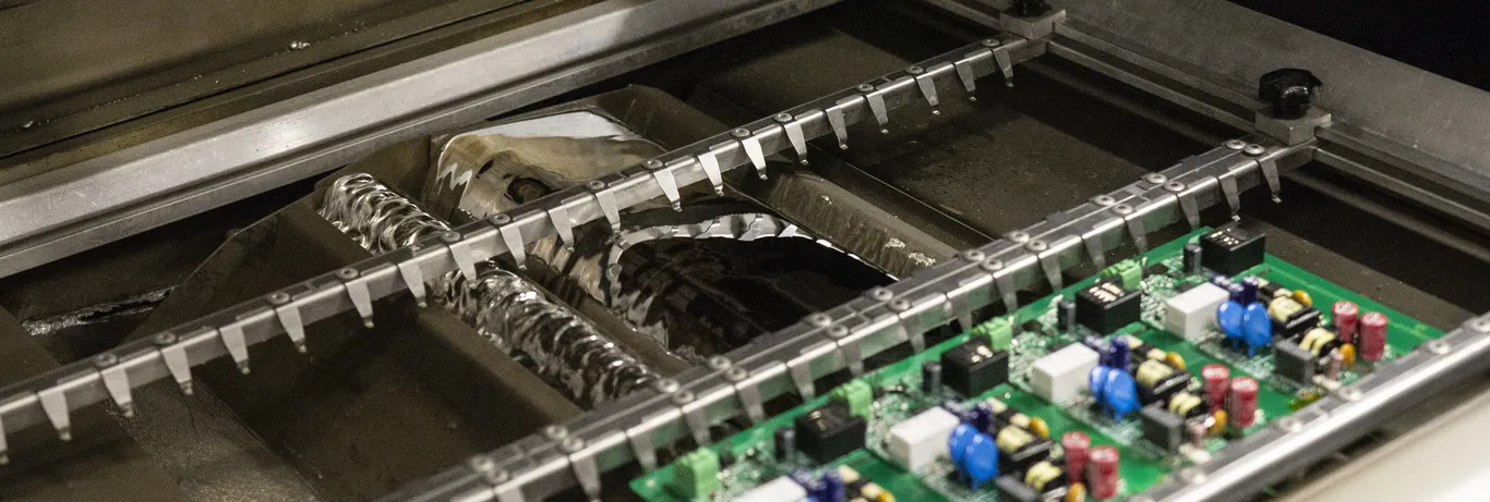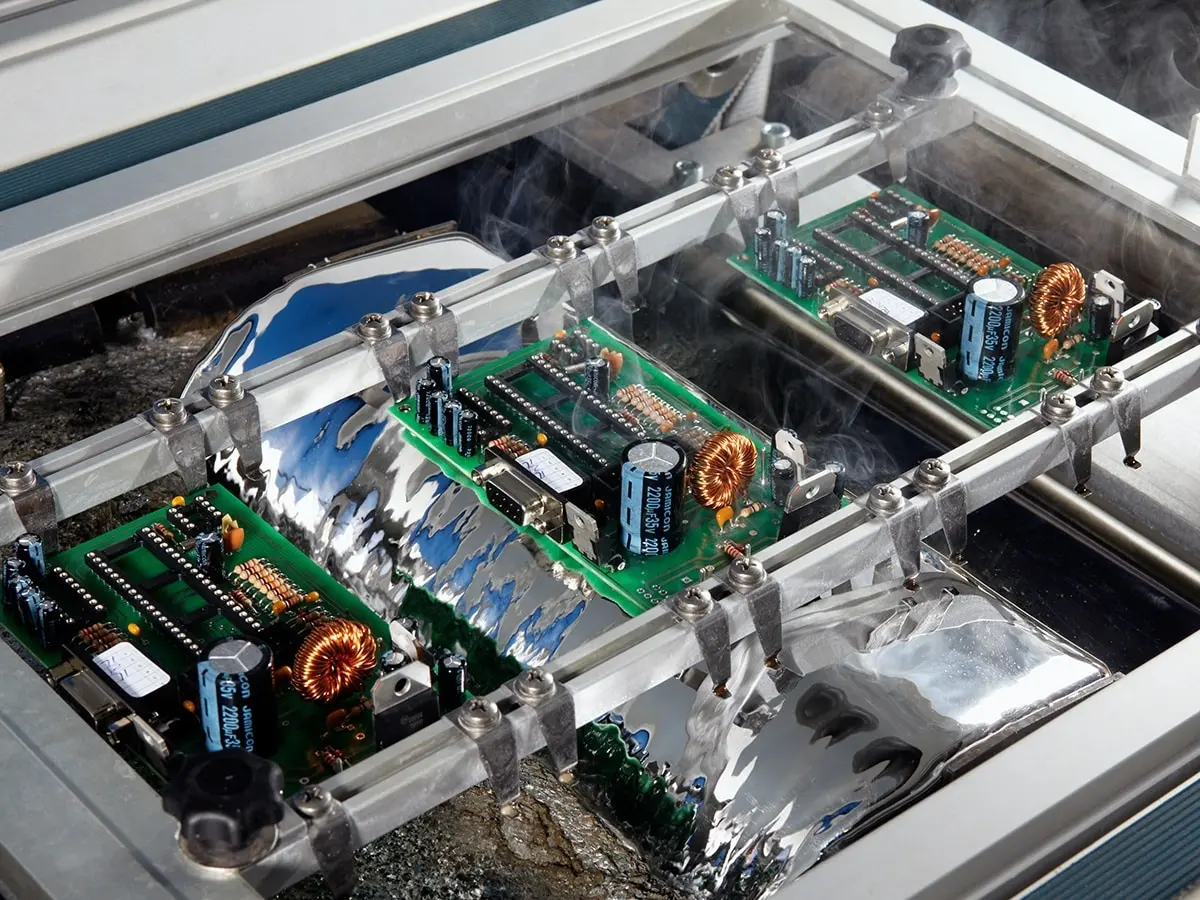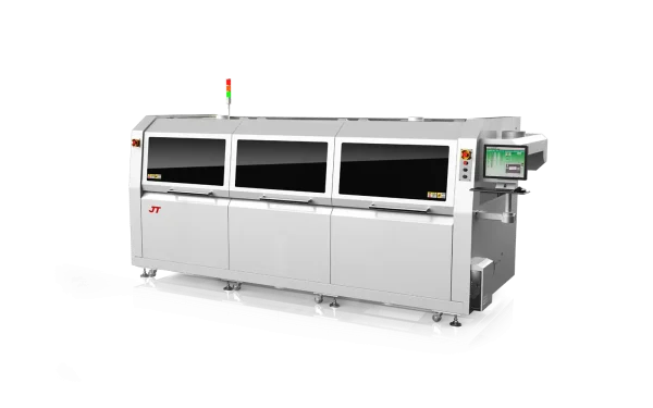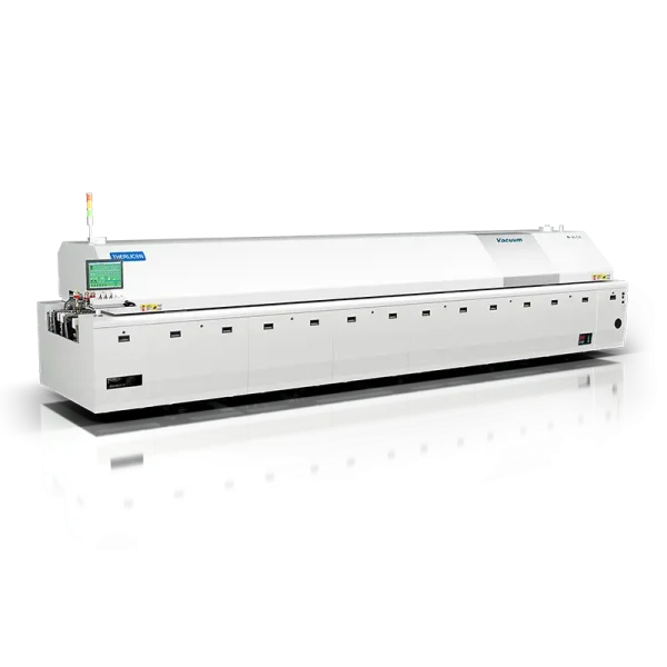

In the wave soldering process of PCB assembly, solder beads remaining on the PCB, while not the most serious defect, are a major source of instability and potential quality issues. Solder beads are formed when the printed circuit board (PCB) leaves the molten solder surface. While there are many reasons for solder bead formation, the two main causes are:
1. When the PCB separates from the solder wave, a connecting solder wire is pulled between the component leads and pads/pads on the PCB and the molten solder pool surface, much like cheese pulling. When this wire continues to stretch and eventually breaks and springs back to the lead or pad, it can easily cause short circuits between adjacent solder joints. The solder falling back into the solder pool will splash onto the PCB, forming solder beads. Secondly, some molten solder may drip directly from the leads into the solder pool, causing splashing. 1. If the adhesion between the solder ball and the PCB surface is less than the weight of the solder ball itself, the solder ball will bounce off the PCB and fall back into the solder pool; otherwise, it will remain on the PCB.
2. At the moment the PCB is removed from the molten solder, some gases that were previously surrounded and confined by the large area of molten solder (from ambient air, flux volatiles, moisture generated by high heat, and gases generated by the solder itself) will escape from the weakest point of the enclosure before the solder solidifies, splashing out and carrying away residual solder. If the weight of the solder ball is less than its adhesion to the PCB, it will remain on the PCB surface.
Most of the above reasons can be effectively solved or improved by using a relatively smooth solder mask (solder resist).
Secondly, it is not recommended to use NSMD (non-solder resist-only) pads on the solder surface where the circuit board contacts the solder wave, because areas without solder resist coverage become rougher, making it easier for solder balls to adhere to the PCB surface.
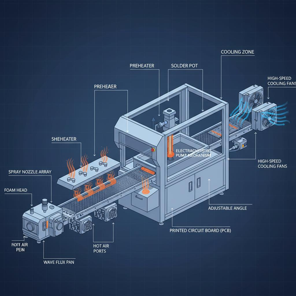
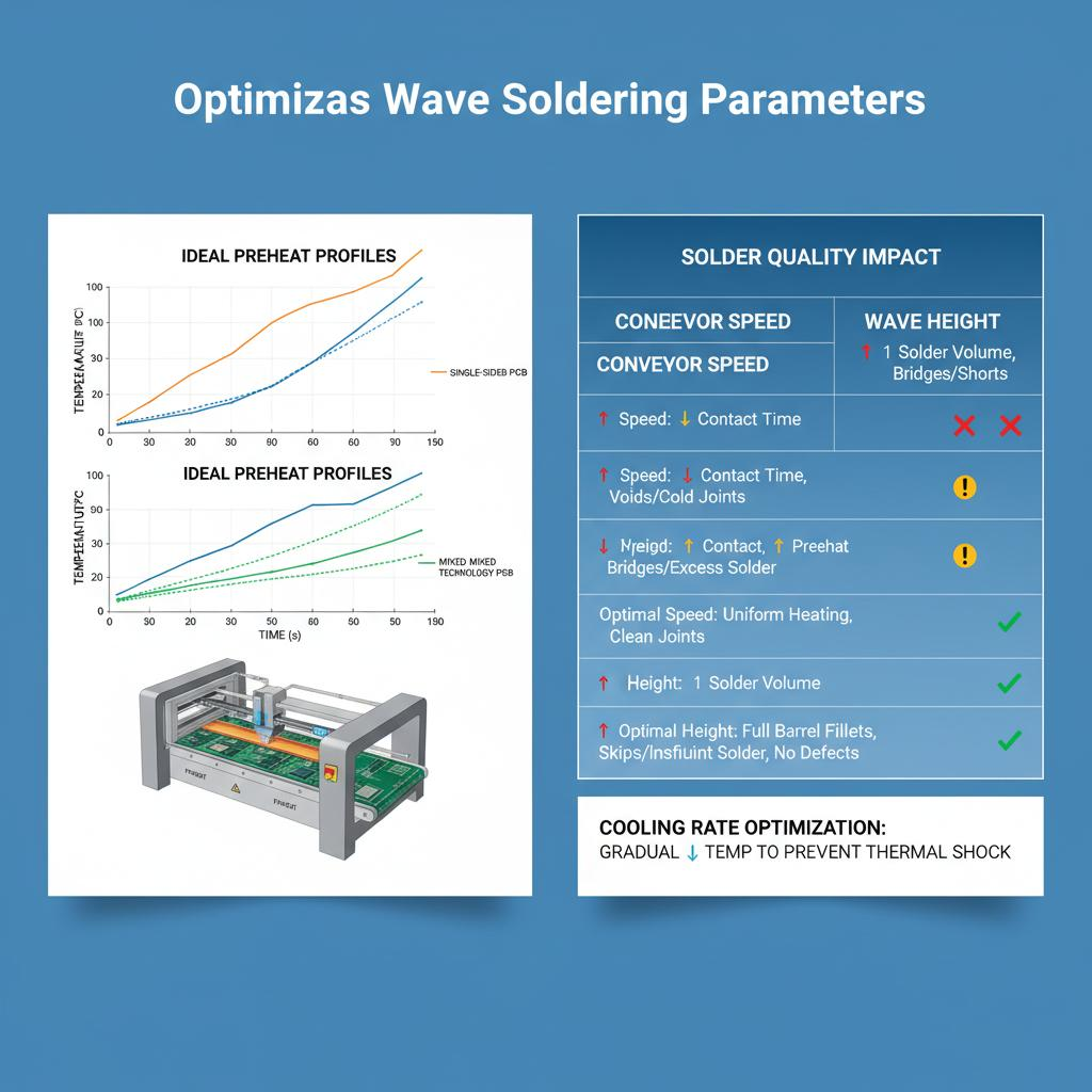
Thirdly, appropriately adjusting the desoldering angle of the wave soldering oven (the angle between the horizontal wave and the track) can also improve the problem of solder ball rebound. Theoretically, lowering the desoldering angle can reduce the distance the molten solder drips from the pins, reducing the force of the splash. However, if the angle is too small, it will hinder the exhaust of the enclosed air. Therefore, only through experimental design can an optimal balance of quality be achieved.
Solder ball formation is also influenced by other factors, such as moisture absorption by the PCB, incomplete flux application, and insufficient preheating. Additionally, improper wave soldering carrier design, causing solder seepage at the edges of the mask opening, is also a possible cause.