As a core piece of equipment in surface mount technology (SMT) for electronic manufacturing, reflow ovens precisely control the temperature profile to melt solder paste and achieve a reliable connection between components and the PCB board. With the continuous miniaturization and high-density development of electronic components, the technological iteration of reflow ovens is accelerating, resulting in various types to meet different needs. The following analyzes the main types of reflow ovens from three dimensions: heating method, application scenarios, and technical characteristics.
I. Classification by Heating Method: The Game Between Radiation and Convection
1. Infrared Reflow Ovens
As an early mainstream device, infrared reflow ovens heat the PCB board through infrared radiation, featuring rapid heating and high thermal efficiency. However, their limitations are significant: differences in component color and size can lead to uneven heat absorption, and dark-colored components or large heat sinks are prone to forming “shadow areas,” causing cold solder joints or poor soldering. For example, under simple infrared heating, the temperature of a black IC package with white leads may be 10-15°C lower than the body temperature, requiring overall temperature compensation, but this may damage heat-sensitive components. Currently, infrared soldering ovens have been gradually replaced by composite heating technologies and are still used only in low-cost, simple circuit soldering.
2. Hot Air Reflow Oven
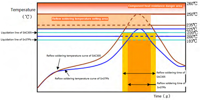
These ovens achieve uniform heating through forced hot air circulation. The hot air is blown out from the upper and lower heating zones, guided by a rectifier plate to form a laminar flow that covers the PCB surface. Its advantages include high temperature uniformity, with temperature differences controllable within ±2℃, making it suitable for high-density, multi-layer board soldering. For example, HELLER’s enhanced heater module further reduces the PCB surface temperature difference by increasing the impeller diameter by 40% and using heat blanket coverage technology, while simultaneously reducing nitrogen consumption by 40%. However, hot air soldering ovens have higher energy consumption, and the strong airflow may displace micro-components such as 0201 chips, requiring adjustment of the airflow speed (typically 1.0-1.8 m/s) to balance heating and component protection.
3. Infrared + Hot Air Composite Soldering Oven
Combining the strong penetrating power of infrared radiation with the high uniformity of hot air convection, it is designed with a 30% infrared + 70% hot air ratio. Infrared preheating provides rapid temperature rise, while the hot air stage eliminates temperature differences, making it particularly suitable for irregularly shaped components or PCBs with mixed materials. For example, under combined heating, the temperature difference between black phenolic packaged ICs and white metal leads can be reduced to within ±3℃, significantly improving soldering yield. This technology was once the mainstream solution in the 21st century, but its market share has been gradually replaced by the maturity of full hot air technology.
4. Vapor Phase Reflow Oven (VPS)
This oven utilizes the boiling point of fluorocarbons (approximately 215℃) to generate saturated vapor, achieving oxygen-free soldering through latent heat release. Its advantages include precise temperature control (±0.5℃), high heat conversion efficiency (200-300W/m²K), and the ability of vapor to penetrate any corner of the PCB, eliminating shading effects. However, the solvent cost is high (approximately $500/L), and chlorofluorocarbons (CFCs) damage the ozone layer. The international community has gradually phased out this technology, retaining its application only in specialized fields such as aerospace.
II. Classification by Application Scenarios: From Mass Production to Precision Repair
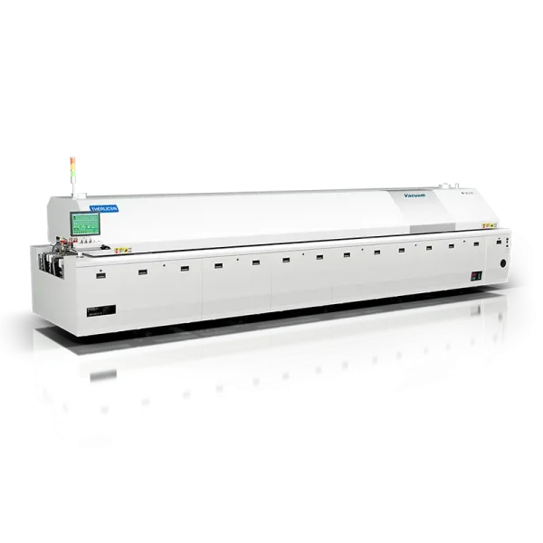
1. Mass Production Soldering Furnaces
Primarily using full-hot air soldering furnaces, these are equipped with 8-12 independent temperature zones, supporting heating channels up to 1.5 meters long, enabling continuous production of 3000 PCBs per hour. For example, the HELLER 450℃ high-temperature custom furnace is designed for MINI LED chip packaging, offering flexible multi-zone temperature adjustment (±1℃ accuracy) and a stepped cooling zone (0-5℃/s adjustable slope) to meet high-density soldering requirements.
2. Precision Repair Soldering Furnaces
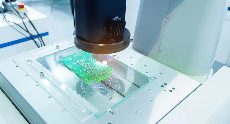
Including localized heating equipment such as laser reflow soldering and focused infrared reflow soldering. Laser soldering furnaces utilize CO₂ or YAG laser beams focused to a 0.1mm² area for single-point soldering, achieving energy densities up to 10⁶W/cm², suitable for BGA rework or military electronic device soldering. Focused infrared soldering furnaces use optical systems to narrow the infrared radiation range, reducing the thermal impact on surrounding components, and are commonly used in laboratory-level prototype development.
III. Classification by Technological Upgrade: From Traditional to Intelligent
1. Traditional Reflow Ovens
Relying on mechanical temperature control and fixed airflow design, temperature profile adjustment requires manual parameter input, resulting in changeover times of up to 2 hours. For example, early hotplate reflow ovens heated ceramic substrates via heat-conducting conveyor belts, offering a simple structure but poor temperature uniformity (±10℃), suitable only for single-sided thick-film circuit soldering.
2. Intelligent Reflow Ovens
Integrating Industry 4.0 technologies, supporting MES/ERP system integration, and capable of uploading 2000 sets of process parameters to the cloud in real time. For example, the HELLER enhanced reflow oven is equipped with an intelligent management system that optimizes temperature profiles through AI algorithms, reducing changeover time to 30 minutes while dynamically adjusting nitrogen consumption, reducing operating costs by 15%.
Conclusion
The technological evolution of reflow ovens has consistently revolved around three core requirements: temperature uniformity, component protection, and production efficiency. From infrared to hot air, from mass production to precision repair, from mechanical control to intelligent management, each technological breakthrough has propelled electronic manufacturing towards higher precision and lower costs. In the future, with the widespread adoption of wide-bandgap semiconductor devices such as silicon carbide (SiC) and gallium nitride (GaN), reflow ovens will need to further overcome technical bottlenecks such as high temperature (>450℃) and high speed (>0.5m/s conveying) to provide key support for the next generation of electronics industry.