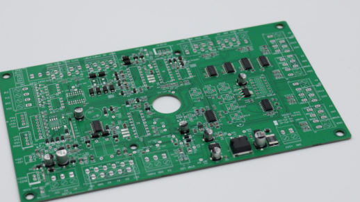
In modern electronics manufacturing, 3D solder paste inspection, as a key technology to ensure the soldering quality of electronic products, has become a crucial link in ensuring product reliability due to its unique advantages.

High-Precision 3D Measurement, Accurately Capturing Details
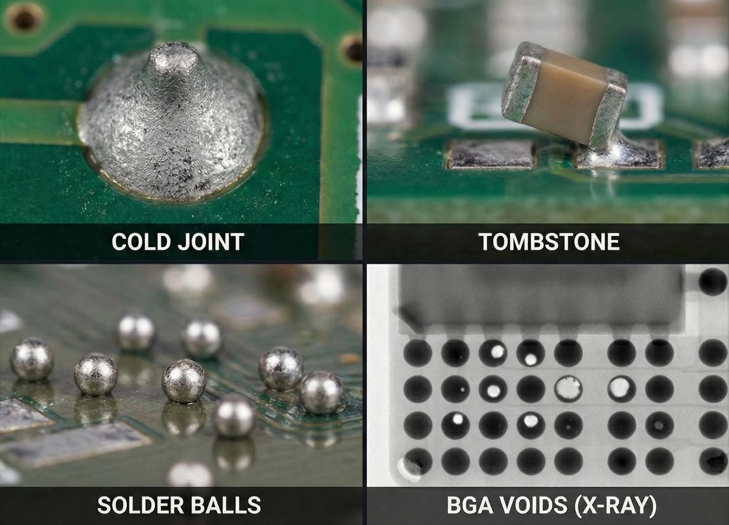
Traditional 2D inspection can only obtain the projection information of solder paste on a plane, making it difficult to accurately measure key 3D parameters such as solder paste thickness and volume. 3D solder paste inspection, however, utilizes advanced technologies such as laser scanning and structured light projection to perform omnidirectional scanning of the solder paste from multiple angles, constructing a precise 3D model. This model allows for accurate measurement of parameters such as solder paste thickness, volume, and area, with precision down to the micrometer level. For example, in the manufacturing of high-end smartphone motherboards, the chip pin spacing is extremely small, and the requirements for solder paste thickness and volume are extremely stringent. 3D inspection can accurately control these parameters, avoiding problems such as short circuits due to excessive solder paste or cold solder joints due to insufficient solder paste.
Fast and Efficient Inspection, Improving Production Efficiency
In the context of large-scale production in electronics manufacturing, time is money. 3D solder paste inspection equipment has high-speed scanning and data processing capabilities, enabling the inspection of an entire circuit board in a short time. Taking an automated production line as an example, 3D inspection equipment can seamlessly integrate with printers, pick-and-place machines, and other equipment to achieve real-time online inspection. Immediately after solder paste printing, the solder paste is inspected. If problems are found, printing parameters can be adjusted promptly, preventing batch defects and significantly improving production efficiency while reducing time and cost waste caused by rework.
Comprehensive Defect Identification, Ensuring Product Quality
3D solder paste inspection can identify various types of solder paste defects. In addition to common two-dimensional defects such as misalignment and bridging, it can also detect three-dimensional defects such as uneven solder paste thickness and abnormal volume. For example, the presence of air bubbles or impurities in the solder paste can cause changes in local thickness and volume; 3D inspection can sensitively capture these subtle changes and promptly identify potential quality problems. Through comprehensive defect identification and analysis, companies can trace the problematic stages in the production process, such as printing pressure and stencil cleanliness, and thus make targeted improvements to enhance the overall product quality.
With its high precision, speed, efficiency, and comprehensive defect identification, 3D solder paste inspection provides reliable quality assurance for the electronics manufacturing industry. As electronic products continue to become smaller and denser, 3D solder paste inspection technology will play an increasingly important role, driving the electronics manufacturing industry toward higher quality and higher efficiency.