In the SMT (Surface Mount Technology) electronics manufacturing field, wave soldering is a core process for the mass soldering of through-hole components and mixed-assembly circuit boards. It quickly and reliably connects multiple solder joints by bringing the PCB board into contact with the wave peaks formed by molten solder. With its high efficiency and stability, it is widely used in PCBA assembly for electronic products such as automotive electronics and industrial control. Below is a detailed breakdown of its working principle and process flow.
I. Core Working Principle of Wave Soldering
The core of wave soldering is to achieve a stable bond between the solder and the components and PCB board through the synergy of physical action and metallurgical reaction. This can be divided into three key parts:
1. Wave Peak Generation: Lead-free tin alloy (such as SAC305) in the solder bath is heated to 260-270℃ and molten. It is then pumped upwards by a mechanical impeller pump, and controlled by nozzles and baffles to form a double wave peak composed of turbulent and laminar waves. The former has a strong impact, while the latter is stable, adapting to different soldering requirements.
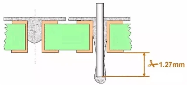
2. Physical Wetting: The PCB board is swept across the wave crest at a 5-7° angle and a stable speed. Molten solder spreads across the pads due to surface tension, and simultaneously climbs and fills through-holes vias through capillary action, enveloping component leads, laying the foundation for soldering.
3. Metallurgical Bonding: Pre-applied flux removes oxides from the metal surface. At high temperatures, the solder alloys with the copper pads and component leads, forming an intermetallic compound layer. After the solder cools and solidifies, a solder joint with both electrical connection and mechanical strength is formed.
II. Standard Wave Soldering Process
Wave soldering is a continuous and precise process. Parameter deviations at any stage can lead to soldering defects, requiring strict adherence to the following steps:
(I) Pre-treatment
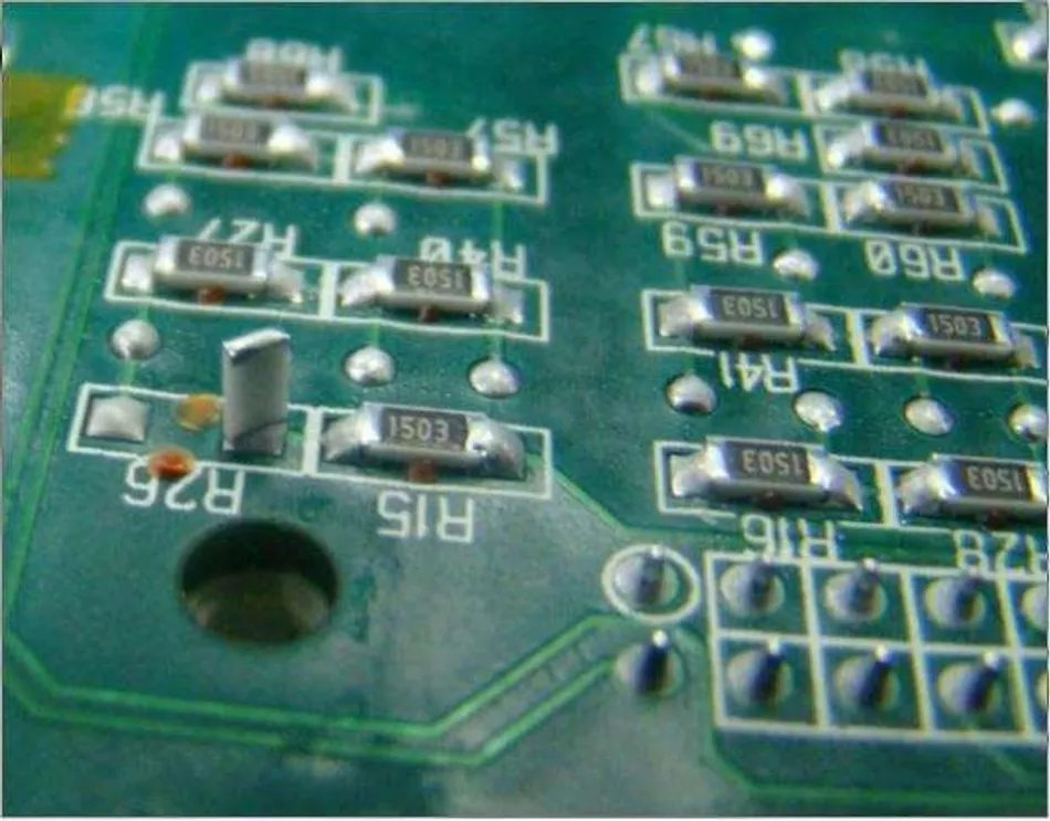
First, accurately insert the through-hole components into their corresponding positions on the PCB. For mixed-assembly boards, use a high-temperature carrier to protect the surface-mount components. Then, uniformly apply flux using a spray device. This removes impurities from the metal surface, reduces solder surface tension, and prevents secondary oxidation during soldering.
Wave Soldering Flux Spraying Process
(The image shows the PCB board being uniformly coated with flux by a spray device as it passes through the conveyor rails.)
(II) Gradient Preheating
The flux-coated PCB enters a four-stage preheating zone, where it is heated to 100-140℃ via hot air convection. This step evaporates the solvent in the flux, activating its activity, and simultaneously reduces the temperature difference between the PCB and the molten solder, preventing the PCB from cracking due to thermal shock and also preventing solder ball splattering during soldering.
(III) Core Wave Soldering
The preheated PCB enters the soldering zone. First, a turbulent wave passes through the component shadowing effect, ensuring solder wetting at densely packed pins; then, a laminar flow wave corrects the solder joint shape and removes excess solder. At this stage, precise control of the 2-5 second contact time is required to ensure sufficient metallurgical reaction without damaging components.
(IV) Cooling and Post-Inspection
After leaving the wave soldering station, the PCB enters a forced air cooling zone, where the solder joints solidify rapidly, preventing structural loosening. After cooling, excess leads are trimmed manually or by equipment. AOI inspection is used to check for defects such as bridging and cold solder joints. Defective solder joints are promptly repaired. Some high-requirement products also require additional electrical performance testing.
III. Wave Soldering Process Optimization and Equipment Adaptation
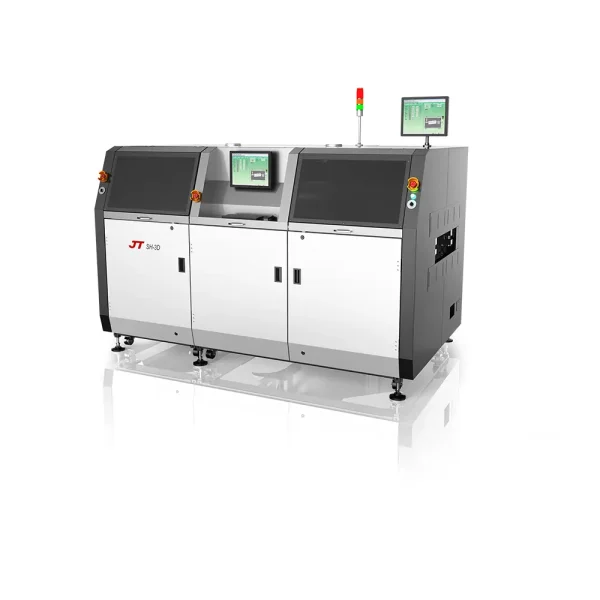
With the increasing density of electronic components, the stability and adaptability requirements of wave soldering are higher. Companies need to regularly maintain the purity of the solder pot, calibrate the wave height, and optimize the preheating profile. JT wave soldering equipment perfectly meets these needs. With its precise parameter control and high reliability, the series of equipment has become the preferred choice for many manufacturing companies to improve soldering quality and reduce defect rates, driving the continuous upgrading of SMT soldering processes towards high efficiency and stability.