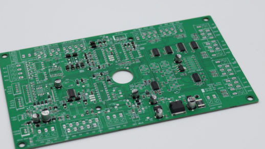
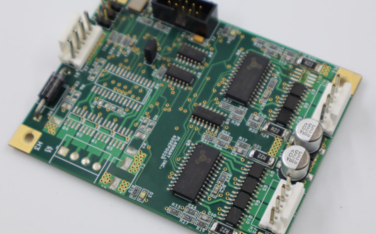
In SMT processes, solder paste printing is a crucial step. Studies show that 80-90% of SMT defects originate from this stage. This is where SPI comes in – acting as a rigorous “quality guardian.” Placing SPI after solder paste printing but before component placement allows for significantly earlier defect detection, saving considerable time and money compared to discovering problems after reflow soldering. As components such as 0201 packages become smaller, requiring more precise solder paste printing, the importance of SPI is increasingly evident. Early detection of problems reduces rework costs and simplifies maintenance.

(1) High Detection Accuracy
Most SPI machines use advanced 3D imaging technology to accurately measure parameters such as solder paste height, volume, and area. Some high-end SPI machines have a Z-axis resolution of up to 0.6 micrometers and a height accuracy of 2 micrometers, capturing even the smallest deviations or defects during solder paste printing.
(2) Comprehensive Detection Capabilities
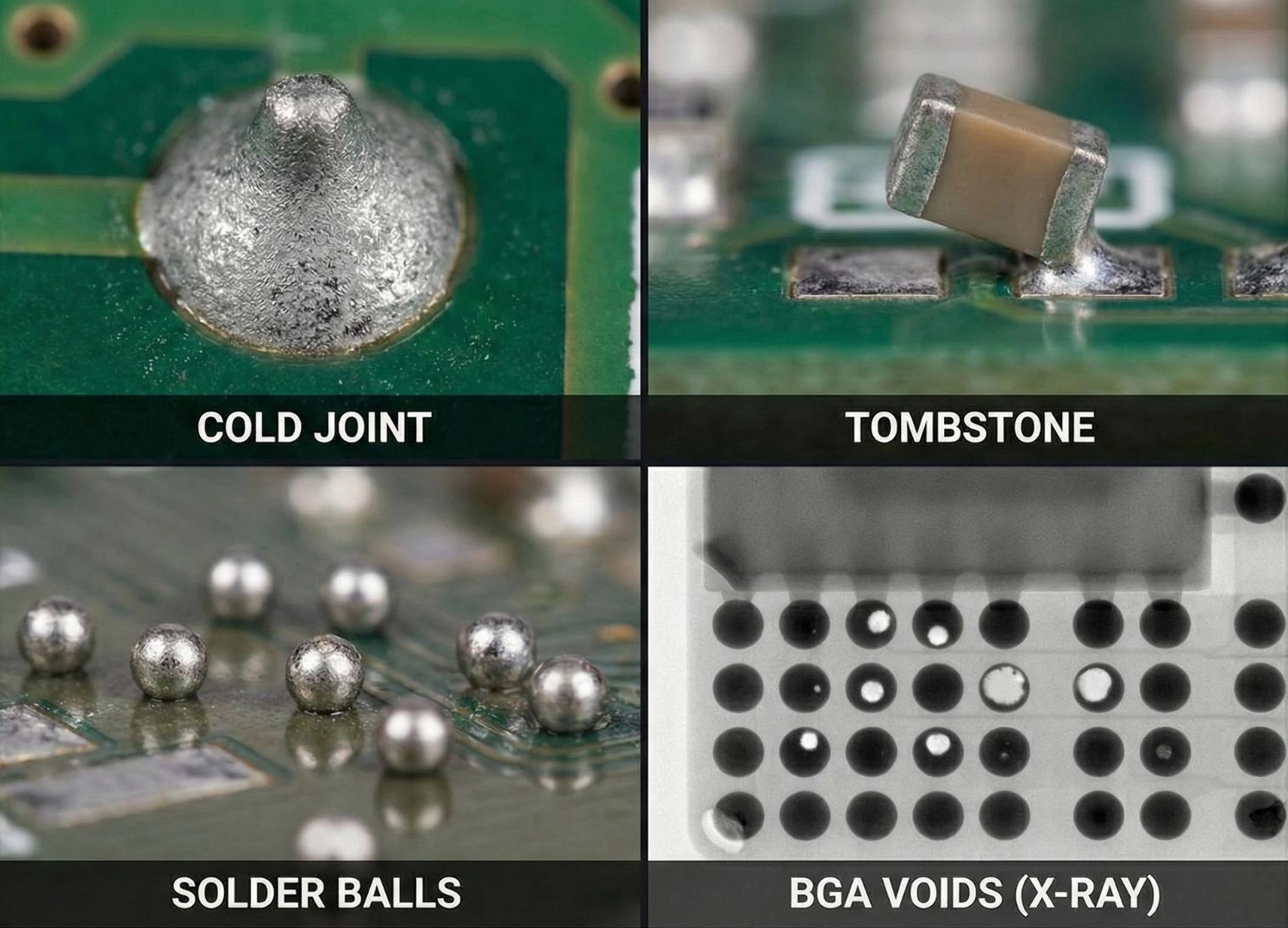
SPI measures more than just basic parameters. It can also detect short circuits, misalignments, deformations, bridging, insufficient solder, and other defects. With this detailed data, operators can adjust printing parameters instantly to improve processes.
(3) Easy to operate
Most SPI machines have a Windows interface, so operators can easily master operation with minimal training. Measurement data can be saved and printed, making it easy to track and review production metrics.
(4) Excellent stability
High-quality SPI machines are manufactured with a focus on stability. Their repeatability and reproducibility (GR&R) are excellent, ensuring consistent and reliable measurements of solder paste thickness, area, and volume.
3. SPI Verification Methods
(1) Laser Inspection
- Point laser: Early laser inspection used point lasers with CCD imaging, but this method was slow because it required X and Y positioning.
- Scan line laser: To improve speed, point lasers were replaced by scan line lasers. This type of laser can quickly scan the solder paste, collecting a large number of data points for more thorough inspection.
(2) Stripe Light Inspection
Another common method in SPI is stripe light inspection, which involves projecting a stripe pattern onto the solder paste surface. By analyzing the distortion and reflection of the stripes, the system can calculate the height and shape of the solder paste. This method also performs well in terms of speed and accuracy.
Other methods include 360° profile measurement, coordinate mapping, structured light, and dual-lens stereo vision, but they are less commonly used in on-the-fly testing due to speed limitations.
4. SPI Verification Standards
(1) Equipment Capacity Standards
- PCB Handling Capacity: SPI machines typically handle PCBs from 50x50mm to 450x535mm (single rail) or 450x250mm (double rail). They can measure PCB thicknesses from 0.4 to 4 mm and compensate for PCB warpage up to ±5 mm.
- Accuracy Requirements: Camera resolution is typically 25 micrometers or higher. For high-precision components, such as 0.3/0.35mm pitch or 01005 devices, a resolution of 20 micrometers is required. The minimum measurable size for square components is typically 200 micrometers, and for round components, it is typically 250 micrometers.
(2) Manufacturing Process Standards
- Solder Offset Specifications: For 01005 components, the solder paste offset must be less than 30% of the standard pad length and 30% of the pad width. For non-01005 components, the offset must be less than 35%.
- Solder Volume Specifications: The volume and area of the solder paste are based on the theoretical opening of the stencil and have corresponding standards. If the specifications are exceeded, cleaning and adjustment are required.
First, the SPI machine takes an image of a flawless circuit board (the “standard” sample) for reference. The board will use this as a reference for evaluation. The inspection method may vary depending on the technology used. For example, in laser inspection, a scanning laser follows a predetermined path on the PCB solder paste. The laser reflection varies depending on the height difference between the solder paste and the surrounding PCB, allowing the machine to accurately calculate the solder paste height. The system scans the entire board to collect data such as solder paste height, volume, and area.
After inspection, the SPI device compares the data with preset standards. If any defects are detected, it triggers an alarm and provides detailed information about the defective area for quick resolution.
Conclusion
SPI is an indispensable part of the SMT process. Understanding its role, characteristics, inspection methods, standards, and workflow helps manufacturers better utilize SPI equipment, improve product quality, reduce production costs, and enhance competitiveness. With the continuous development of electronic manufacturing technology, SPI will continue to innovate and advance, providing stronger support for the high-quality production of electronic products.