A key step in ensuring high-quality results is solder paste inspection (SPI). But what exactly is SPI, and why is it so important? SPI is a process of inspecting the solder paste deposit on a printed circuit board (PCB) before components are placed and soldered. It verifies critical factors such as solder paste volume, height, area, and alignment to detect defects early. This prevents costly rework and ensures the reliability of electronic products.

What is Solder Paste Inspection (SPI), and why is it important?
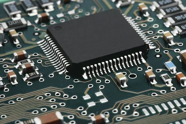
Solder paste inspection (SPI) is a quality control step in the Surface Mount Technology (SMT) process for PCB assembly. During PCB manufacturing, solder paste (a mixture of tiny solder particles and flux) is applied to the pads of the circuit board to establish a connection between components and the PCB. Incorrect solder paste application can lead to poor connections, component misalignment, or even complete product failure.
SPI uses specialized machines to inspect the solder paste deposit immediately after it has been printed onto the PCB. It can detect problems such as insufficient or excessive solder paste, incorrect height, uneven coverage, or misalignment. By identifying these issues early, SPI reduces the risk of defects during the reflow soldering process, thereby saving time and money. In fact, research shows that up to 70% of soldering defects originate from improper solder paste application, making SPI a crucial inspection point.
How does solder paste inspection work?
The SPI process is typically performed immediately after solder paste is printed onto the PCB using a stencil. Specialized SPI machines use advanced imaging technology to analyze the paste deposit. These machines capture detailed data about the solder paste and compare it to predefined standards to ensure quality.
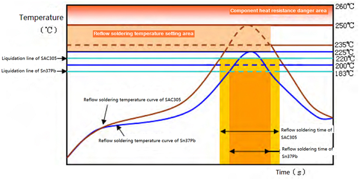
Traditional 2D SPI systems rely on cameras to capture planar images of the solder paste, detecting basic issues such as missing or misaligned paste. However, modern 3D SPI systems go further. They use laser or structured light technology to create a three-dimensional view of the solder paste deposit. This allows for precise measurement of key parameters such as solder paste volume, height, and area, providing a more accurate quality assessment.
For example, a 3D SPI machine might measure a solder paste deposit with a volume of 120 cubic micrometers, a height of 150 micrometers, and an area coverage of 90% of the pads. If any of these values are outside acceptable ranges (e.g., a volume below 100 cubic micrometers), the system flags it as a potential defect. This level of detail helps manufacturers address problems before they escalate.
Key Parameters for Solder Paste Inspection
SPI focuses on several key metrics to ensure proper solder paste application. Let’s break down each parameter and its importance in PCB manufacturing.
1. Solder Paste Volume
Solder paste volume refers to the total amount of solder paste deposited on each pad. Too small a volume results in weak solder joints, while too large a volume causes bridging, where excess solder connects adjacent pads and creates a short circuit. 3D SPI systems measure solder paste volume in cubic micrometers to ensure it falls within a target range, typically between 100 and 150 cubic micrometers for standard SMT pads. Maintaining the correct volume is crucial for reliable electrical connections.
2. Solder Paste Height
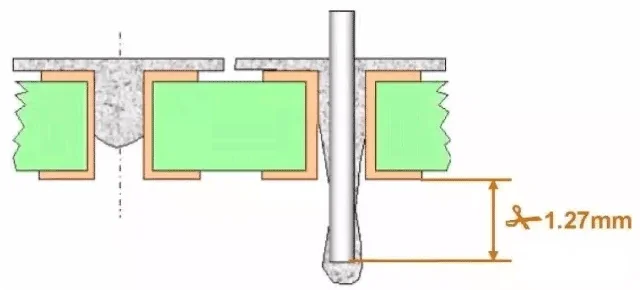
Solder paste height is the vertical thickness of the solder paste deposit, typically measured in micrometers. Too low a height (e.g., below 120 micrometers) may not provide enough material for a strong bond, while too high a height (e.g., above 180 micrometers) can lead to uneven soldering. SPI ensures consistent solder paste coverage across the entire pad, typically targeting a range of 130-160 micrometers for most applications.
3. Solder Paste Area
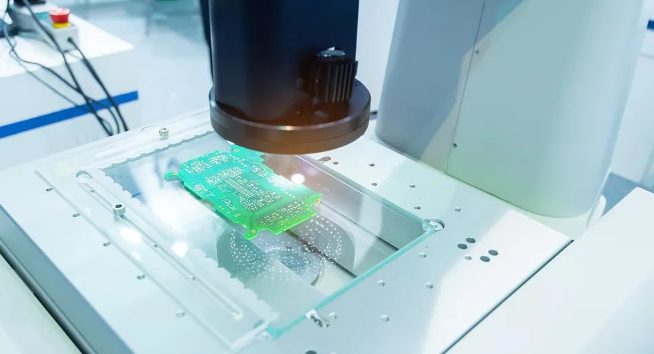
Solder paste area refers to how much solder paste covers the pads. Ideally, the paste should cover 90-100% of the pad surface. Coverage below 80% can lead to insufficient contact with component leads, resulting in poor soldering. 3D SPI systems provide precise area measurements to detect any gaps or uneven distribution early on.
4. Solder Paste Alignment
Alignment refers to the precision with which the solder paste is positioned on the pads. Misalignment (solder paste offset exceeding 25 micrometers) can cause components to shift during reflow soldering, leading to connection defects. SPI machines use high-resolution imaging to detect even slight misalignments and ensure the paste is centered on each pad.
Challenges in Solder Paste Inspection and How to Overcome Them

While SPI is a powerful tool, it is not without its challenges. A common problem is false alarms, where the system marks a deposit as defective even when it is acceptable. This can occur due to lighting conditions or surface reflections on the PCB. To minimize false alarms, manufacturers can adjust the sensitivity settings of the SPI machine and ensure consistent lighting throughout the inspection process.
Another challenge is inspecting complex PCB designs with varying pad sizes and shapes. For example, a board with both high-power pads and tiny 0.3 mm pitch pads may require different inspection parameters. Customizable 3D SPI software that allows for pad-specific settings can help address this issue.
Finally, the initial cost of SPI equipment can be high, with advanced 3D systems typically costing between $50,000 and $150,000. However, the long-term savings from reduced rework and increased throughput (sometimes by 10-20%) usually justify the investment.
Why SPI is crucial for high-quality PCB manufacturing: Solder paste inspection is the cornerstone of PCB manufacturing quality control. By carefully inspecting the volume, height, area, and alignment of the solder paste, SPI ensures reliable solder joints and minimizes defects. With the precision of 3D SPI technology, manufacturers can identify problems early, improve yield, and meet the stringent requirements of modern electronics.