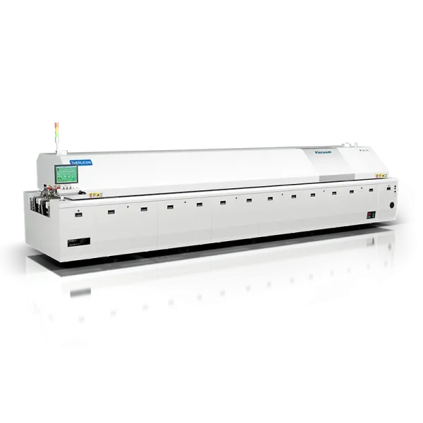
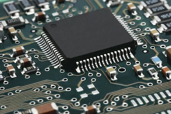
In the electronics manufacturing industry, wave soldering, as a classic soldering technology, has long served the mission of efficiently connecting through-hole components to PCBs (Printed Circuit Boards). Although the rapid development of Surface Mount Technology (SMT) in recent years has given reflow soldering more prominence, wave soldering, with its unique advantages and continuous technological innovation, still maintains its important position in the electronic assembly field and demonstrates broad development prospects.

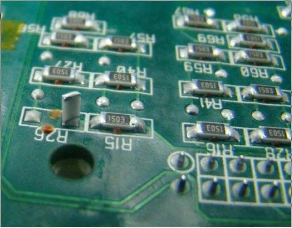
As electronic products increasingly move towards miniaturization and high density, the requirements for soldering processes are becoming increasingly stringent. Wave soldering technology has not stagnated but has actively adapted to market demands, continuously optimizing and upgrading. For example, by introducing a nitrogen-protected environment, oxidation reactions during the soldering process are effectively reduced, improving solder joint quality; selective wave soldering technology allows for precise soldering of specific areas, avoiding bridging or cold solder joint problems that may occur with traditional wave soldering, making it particularly suitable for assembling highly complex, high-density PCBs.
Driven by the wave of intelligentization and automation, wave soldering equipment is also undergoing intelligent transformation. Modern wave soldering systems integrate advanced sensor, machine vision, and data analysis technologies, enabling real-time monitoring and automatic adjustment of welding parameters, significantly improving production efficiency and welding consistency. Simultaneously, through integration with upper-level management systems such as MES (Manufacturing Execution System), wave soldering equipment can seamlessly integrate into intelligent manufacturing systems, achieving transparency and traceability in the production process, providing powerful data support and management convenience for electronics manufacturing companies.
Furthermore, increasingly stringent environmental regulations are driving the development of wave soldering technology towards greener practices. The widespread application of lead-free solder and the effective treatment of waste gas and slag during the soldering process demonstrate the positive response of wave soldering technology to environmental protection.
Looking to the future, with the rapid development of emerging fields such as 5G, the Internet of Things, and new energy vehicles, the demand for electronic products will continue to grow, providing a vast market space for wave soldering technology. At the same time, continuous technological progress and innovation will drive wave soldering towards higher precision, higher efficiency, greater intelligence, and greater environmental friendliness, continuously leading the welding technology innovation in the electronics manufacturing industry.
In conclusion, wave soldering, as a cornerstone technology in the field of electronic manufacturing, will continue to write its glorious chapter through continuous technological innovation and market expansion.