In surface mount technology (SMT), reflow soldering is a process that melts solder paste to permanently attach electronic components to a printed circuit board (PCB). Proper reflow soldering ensures the quality and reliability of electronic products.
This guide explains what reflow soldering is and its process flow, reflow profiles, design considerations (such as PCB edge guides), and advanced reflow soldering methods (including nitrogen reflow soldering and vacuum reflow soldering), and introduces inspection methods before and after reflow soldering.

What is Reflow Soldering?
Reflow soldering uses hot air to melt solder paste and solder surface mount components (SMDs) onto the PCB.
During the SMT assembly process, a solder paste printer applies solder paste to the PCB pads, an SPI inspection machine inspects the solder joints, three pick-and-place machines place the SMD components onto the solder paste, an AOI inspection machine checks the component placement, the assembled circuit board is controlled-heated in a reflow oven, and finally, a second AOI inspection machine checks the soldering quality. For hidden solder joints, X-ray inspection is also required.
As the solder pads pass through the reflow oven, the solder paste melts and, at its peak melting point, bonds with the PCB surface coating and SMD leads, forming a strong metallurgical bond between the SMD and PCB pads. Upon cooling, the solder joint hardens, permanently securing the component.
Reflow soldering is a widely used soldering method in electronic assembly due to its advantages:
Repeatable and automated
Capable of handling fine-pitch devices (01005, 0201, 0402, BGA, CSP, QFN)
Compatible with prototyping and mass production
Reliably forms consistent solder joints
Reflow Soldering Process
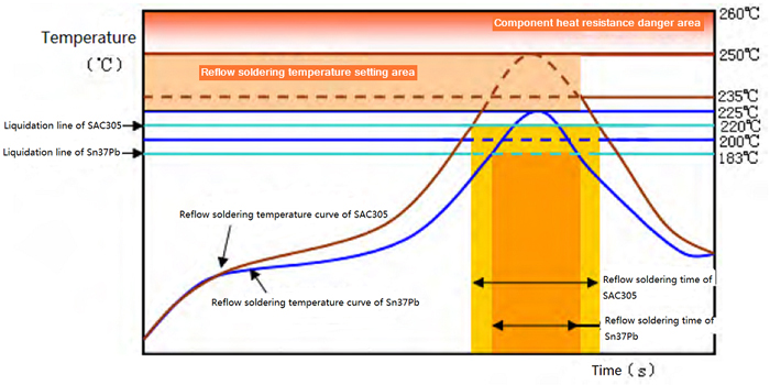
PCBONLINE’s reflow ovens have 10 temperature zones, and the reflow process can be programmed according to reflow profiles designed by our engineers.
The reflow profile defines how the temperature changes inside the reflow oven. It ensures that the activation, melting, and cooling processes of the solder paste proceed correctly without damaging the components.
A typical reflow soldering process includes four main stages:
1. Preheating (Heating Up)
To avoid thermal shock, the PCB board is heated gradually. Flux activation also begins at this stage.
2. Immersion (Thermal Equilibrium)
For each prototype PCB assembly project, a solder paste stencil for SMT assembly is also prepared.
3. Reflow (Peak Zone)
Temperature is stabilized to ensure uniform heating of the PCB board. This reduces voids and eliminates solder splatter.
4. Cooling
Controlled cooling allows the solder to solidify. Too rapid cooling can lead to thermal stress, while too slow cooling can result in insufficient solder joint strength.
Preheating, simmering, and reflow soldering are all part of the reflow soldering heating process. Temperature changes during heating and cooling must be strictly controlled to avoid defects such as solder bridging, tombstoning, or component cracking.
Reflow Soldering PCB Design Considerations
The success of reflow soldering depends on more than just the reflow profile. Proper PCB design plays a crucial role in achieving reliable soldering, including edge guides, SMT stencil design, and component orientation.
1. Edge Guides for PCB Clamping
During reflow soldering, the PCB is transported within the reflow oven via conveyor rails or clamping devices. To avoid interfering with pads or components, designers must provide edge guides (or transport rails) on both sides of the PCB.
Standard clearance: 3 mm to 5 mm per side
No copper traces, vias, or components should be placed in this area.
The edge guides are then removed by disassembling the panel.
Without proper edge guides, the PCB may become misaligned or components may be damaged during reflow soldering.
2. SMT Stencil Design
The solder paste stencil must precisely match the pad dimensions. Don’t worry, SMT stencil design isn’t your job; PCBONLINE has included it in our free Design for Manufacturing (DFM) service. We have extensive experience in SMT stencil design. Our stencil design techniques are as follows:
Fine-pitch ICs and Quantum Dot Packages – To minimize stress concentration, we design the aperture ends with rounded corners.
BGAs and Ultra-small Passive Components (0402, 0201) – Square openings are used to achieve uniform solder ball formation.
QFN Ground Pads – A cross-shaped (“+”) opening pattern is used, maintaining a gap of at least 0.5 mm from the pad edge to prevent solder lumps and ensure effective grounding.
USB, Mini USB, and CF/SD Interfaces – The length of the grounding aperture is increased in a 1:1.2 ratio to increase solder volume. A recessed opening design is used to reduce stress and suppress solder ball formation.
BGA Aperture General Guidelines – The aperture width should be sufficient to allow at least four solder balls to pass through to ensure consistent reflow soldering performance.
3. Component Orientation
Long components such as capacitors, inductors, connectors, and terminals should be placed perpendicular to the conveyor belt direction. This prevents the hot airflow in the reflow oven from lifting or blowing components over, ensuring uniform soldering quality.
Advanced Reflow Soldering Methods
Standard reflow ovens use room temperature air, but oxygen can cause oxidation of solder joints on sensitive components. To address this, PCBOLINE offers two advanced reflow soldering solutions: nitrogen reflow soldering and vacuum reflow soldering.
Nitrogen Reflow Soldering
Nitrogen reflow soldering introduces nitrogen into the reflow oven, reducing oxidation and improving solder joint quality. It is suitable for:
Fine-pitch BGAs and CSPs
High-reliability applications (automotive, aerospace, medical)
Reducing solder voids and wetting issues
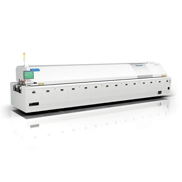
Vacuum Reflow Soldering
Vacuum reflow soldering is an advanced soldering method that applies a vacuum during peak soldering periods. By reducing chamber pressure as the solder melts, residual gases inside the solder are eliminated, significantly reducing solder voids.
Minimizes solder void formation, especially suitable for BGAs, QFNs, and power devices.
Improves thermal and electrical conductivity by ensuring virtually void-free connections.
Enhanced reliability in high-power and high-frequency applications where heat dissipation is critical.
Inspection Before and After Reflow Soldering
How to inspect reflow soldering quality? Visual inspection alone is insufficient. We employ AOI (Automated Optical Inspection) before and after reflow soldering. For concealed solder joints, we also use X-ray inspection.
Pre-reflow AOI: Ensures correct solder paste printing and component placement.
Post-reflow AOI: Inspects solder joint quality, alignment, and polarity.
X-ray Inspection: For concealed solder joints (such as BGA, CSP, and QFN), X-ray inspection is crucial for detecting voids, bridging, or insufficient wetting.
Our dual AOI and X-ray inspection further reduces the risk of rework and ensures long-term product reliability.
Common Reflow Defects
What defects can poor reflow soldering cause? These include:
Tombstone effect—caused by uneven solder paste melting, straightening small components.
Bridging—excessive solder paste or poor stencil design can lead to short circuits.
Voids – Gas trapped in the solder joints creates voids.
Pillow-like wetting – In BGAs, incomplete wetting leads to poor contact.
PCBONLINE guarantees that the PCBAs delivered to you will be free of these reflow soldering defects. We can adjust stencil design, optimize reflow profiles, use nitrogen reflow soldering, and perform 100% functional PCBA testing and aging tests to prevent these defects.
Conclusion: Reflow soldering requires proper reflow profile settings, PCB edge guide design, and SMT stencil installation, as well as AOI and X-ray inspection. With extensive experience in temperature control and SMT soldering, we provide professional reflow soldering and SMT assembly services.