2023-12-08
Did you know that 75% of defects that happen during the solder paste process are due to improper printing of solder paste? The printing process is an essential surface mount assembly process. When a defect occurs, a lot of time and money will be used again to remanufacture.
This is one of the many reasons why buyers are choosing to work with a PCB assembly house equipped with solder paste inspection equipment. That's because this equipment identifies the defect earlier, thus preventing losses.
Uses of a solder paste inspection equipment
SPI machine is set just before the solder paste printing and is done to assist in screening out poor solder printing. It will then trace back to why the defect has happened to minimize the 75% of defects that happen in the process.
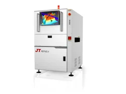
The solder paste inspection equipment is quite similar to the Auto Optical Inspection, AOI- an identification system (Placed behind the SMT surface) that uses optical images to check the board's quality. What makes SPI equipment more outstanding is the additional laser device used to measure the thickness of the solder paste.
Though they function similarly to AOI, the solder paste equipment performs only image inspection on the surface. So, if there is an area covered by any object or something different, an SPI machine cannot perform an inspection in that area.
These are what SPI equipment measures;
- Volume/area of the solder paste printing
- Solder paste printing volume
- Make SPC statistics
- The height and flatness of the solder paste printing
When it comes to identifying the defects, this is what the solder paste inspection equipment can detect;
- The solder paste printing bridges
- The solder paste printing is damaged or defective
- The solder paste printing is bridged
- Shifting of the solar paste printing
- If the solder paste printing is tipped
Methods of inspecting printed PCBs
When inspecting PCBs, there are only two methods: 2D and 3D SPIs.
2D SPI has been the most commonly used for years. However, because of its limited inspection capability, this system cannot check the shape of the solder deposits and volume.
This gap has been closed by 3D solder paste inspection equipment. The 3D SPI checks and measures the volume and shape of the solder deposits. Ideally, this equipment shortens the introduction of any new product because the displayed data is based on measurements, not image interpretation.
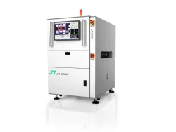
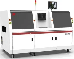
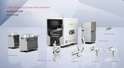
Why JT SPI equipment?
To avoid defects, you need a reliable and well-equipped PCB manufacturer. As mentioned earlier, the most commonly used SPI machines are 2D, which doesn't meet all users' needs because of their capabilities.
However, JT has focused on 3D SPI machines that meet all clients' needs and prevent defects. With this device, you will no longer count losses and waste time only to end up with defective products.
Their machine combines with modern technology, making work easier. Here are the advantages of JT 3D solder paste inspection equipment. For further guidance, JT awaits your call today.
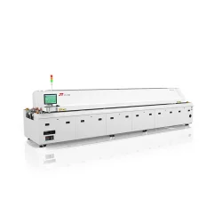
How Wave Soldering Oven Enhances Manufacturing Efficiency?
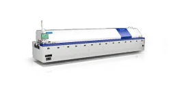
The Ultimate Guide to Wave Machines: How They Work and What are the benefits