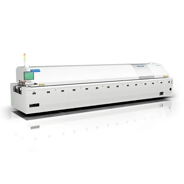
Lead-free hot air reflow ovens are core equipment in the electronics manufacturing industry for surface mount technology (SMT). They achieve precise melting and solidification of lead-free solder through a hot air circulation system, becoming a key tool for precision soldering in modern electronic products. With increasingly stringent global environmental regulations restricting lead-containing materials, lead-free technology has become an inevitable choice for the electronics manufacturing industry, and lead-free hot air reflow ovens are the core carrier of this technological transformation.

I. Technical Background: An Environmental Revolution from Lead to Lead-Free
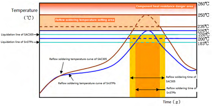
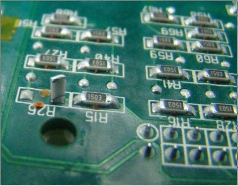
Traditional reflow soldering uses tin-lead alloy solder, with a melting point of approximately 183℃. However, the harmful effects of lead on the environment and human health have prompted the industry to accelerate its lead-free process. Currently, the mainstream lead-free solder is represented by SAC305 (96.5% tin, 3% silver, 0.5% copper), whose melting point has increased to 217-221℃. This places higher demands on the temperature control accuracy, thermal uniformity, and high-temperature resistance of the soldering equipment. Lead-free hot air reflow ovens have successfully overcome the technical bottlenecks of traditional equipment in high-temperature soldering by optimizing the furnace structure, hot air circulation system, and temperature control technology.
II. Core Principle: Precision Control of Hot Air Circulation
The core of a lead-free hot air reflow oven lies in its “hot air circulation + closed-loop temperature control” system. Its working principle is as follows:
1. Hot Air Generation: A motor drives an impeller to rotate at high speed, blowing air or nitrogen onto the heating wire to form uniform hot air;
2. Temperature Closed-Loop Control: Thermocouples monitor the hot air temperature in real time and feed it back to the main control computer. A PID algorithm dynamically adjusts the heating wire power to ensure temperature fluctuations are ≤±1℃;
3. Multi-Layer Hot Air Circulation: The upper and lower heating modules inside the furnace operate independently. Hot air is evenly sprayed onto the PCB surface through a perforated plate, forming laminar heat exchange and preventing localized overheating;
4. Nitrogen Protection (Optional): In high-temperature lead-free soldering, a nitrogen environment can reduce the oxidation rate of solder joints and improve soldering reliability. Some equipment is equipped with a nitrogen concentration closed-loop control system (5-200ppm).
III. Technological Advantages: Three Major Breakthroughs for Lead-Free Soldering
1. Ultra-Wide Temperature Range: The equipment is designed with a maximum temperature of 400℃, covering the melting point and process window of lead-free solder (230-245℃), while traditional lead-containing equipment has a maximum limit of only 300℃.
2. Extremely Uniform Thermal Performance: Utilizing a three-zone temperature distribution system, the longitudinal temperature difference is ≤±1℃, and the lateral temperature difference is reduced by 15% through a small-circulation hot air design, ensuring that large heat capacity components (such as BGA and IGBT) reach soldering temperature synchronously with smaller components.
3. High-Efficiency and Energy-Saving Design: Imported aluminum silicate insulation layer reduces heating time to ≤20 minutes; dual-track dual-speed technology reduces energy consumption by 60%; and the forced air cooling system controls the PCB exit temperature at 38-50℃, preventing thermal stress damage.
IV. Typical Application Scenarios
Lead-free hot air reflow ovens are widely used in high-precision electronic manufacturing:
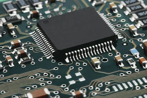
• Smartphone/Computer Motherboards: Soldering micro-components such as 0201 chips and QFN packages, improving yield to over 99.9%;
• Automotive Electronics: Ensuring the reliability of IGBT module solder joints in extreme environments ranging from -40℃ to 150℃;
• LED Packaging: Achieving deformation-free soldering of flexible printed circuit boards (FPCs) using low-temperature solders (such as Sn-Bi alloys);
• Aerospace: Meeting GJB military standards, soldering high thermal conductivity substrates and ceramic components.
V. Technological Development Trends
As the SMT industry moves towards higher density and higher reliability, lead-free hot air reflow ovens are evolving towards intelligence and modularity:
• AI Temperature Profile Optimization: Automatically generates optimal soldering parameters through machine learning, shortening debugging time;
• Multi-Process Compatibility: Supports additional functions such as red glue curing and chip aging, achieving “one machine, multiple uses”;
• Green Manufacturing: Employs a low-VOC flux filtration system, reducing nitrogen consumption by 30%, contributing to carbon neutrality goals.
Lead-free hot air reflow ovens are not only a product of environmental regulations but also a symbol of technological upgrades in electronic manufacturing. Through precise hot air control and material innovation, they provide reliable soldering solutions for cutting-edge fields such as 5G communications, new energy vehicles, and artificial intelligence, becoming a “hidden champion” driving high-quality development in the electronics industry.