Behind the precision circuit boards in smartphones, automotive electronics, aerospace, and other fields, an automated soldering technology called wave soldering is silently supporting the efficient operation of the global electronics manufacturing industry. As a core process of through-hole mounting (THT) technology, wave soldering achieves efficient and reliable connections between component leads and circuit board pads through dynamic waves formed by molten solder, becoming an indispensable “invisible bridge” in modern electronics manufacturing.

Technical Principle: A Perfect Combination of Dynamic Waves and Wetting Soldering
The core of wave soldering lies in using a mechanical or electromagnetic pump to pump molten solder (such as lead-free SAC305 alloy or traditional Sn63Pb37 alloy) from a solder bath, forming a stable upward wave through nozzles. When a pre-assembled circuit board moves uniformly across a wave crest at a specific angle (typically 5-7 degrees) and speed (1-2 meters per minute), molten solder wets the contact surface between the leads and pads. Through surface tension, capillary action, and metallurgical reactions, intermetallic compounds form at high temperatures, eventually solidifying into solid solder joints upon cooling. This process is akin to a “dance of liquid metal,” requiring both wave crest stability and precise control of the circuit board’s movement.
Process Flow: Intricate Collaboration at Each Step
A typical wave soldering process includes six key steps:
1. Flux Coating: Flux is evenly sprayed onto the soldering surfaces of the circuit board using spraying or foaming methods to remove oxide layers and reduce solder surface tension.
2. Preheating: Infrared heating or hot air convection is used to gradually raise the circuit board temperature to 90-100°C, avoiding thermal shock and activating the flux.
3. Wave Soldering: The circuit board is sequentially passed through turbulent waves (to break through the oxide layer) and laminar waves (to form high-quality solder joints), with contact time controlled within 2-5 seconds.
4. Cooling: Forced air cooling or natural cooling allows for rapid solidification of the solder joints, preventing excessive growth of intermetallic compounds that could lead to embrittlement.
5. Cleaning (Optional): Removes residual flux, especially suitable for high-reliability applications.
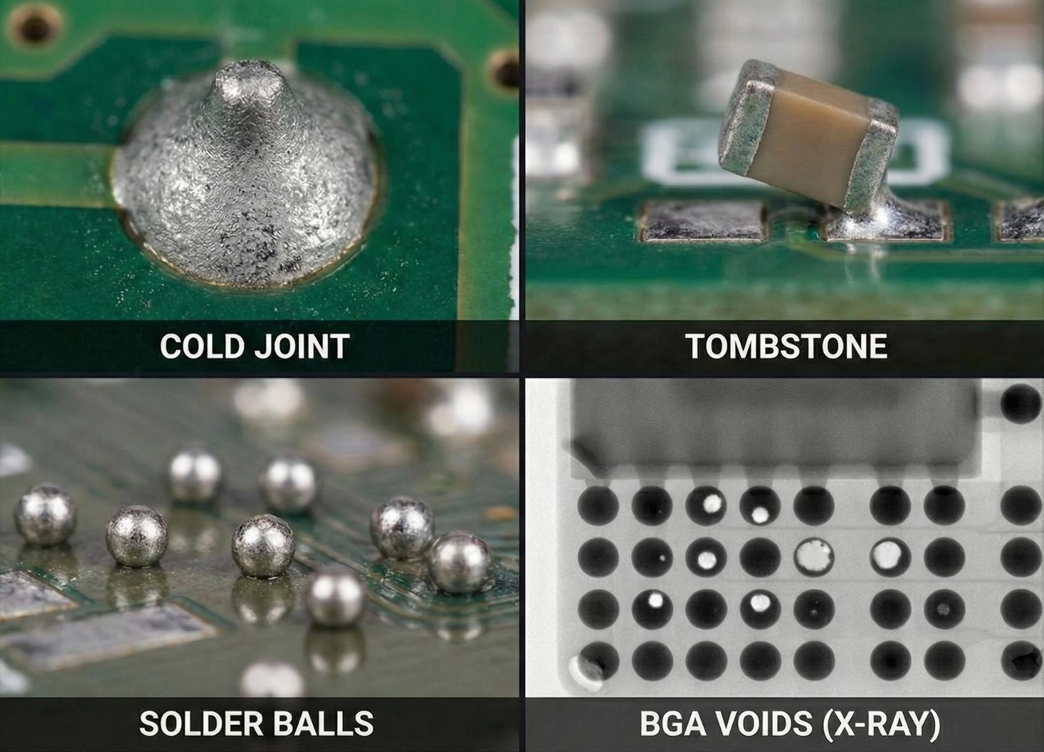
6. Inspection: Solder joint quality is inspected using AOI (Automated Optical Inspection) or X-rays to ensure the absence of defects such as cold solder joints and bridging.
Advantages and Challenges: Balancing Efficiency and Precision
Advantages:
• High-Efficiency Mass Production: Hundreds of solder joints can be soldered in a single pass, suitable for large-scale production scenarios such as televisions and power boards.
• Controllable Costs: Lower equipment investment than reflow soldering, and no need for stencil fabrication, suitable for products with a high proportion of through-hole components.
• Mature Process: After decades of development, parameter control (such as wave height and conveyor speed) is highly standardized.
Challenges:
• Miniaturization Limitations: Bridging is prone to occur with tiny components like 0201 solder balls or high-density circuit boards, requiring selective wave soldering technology.
• Lead-Free Difficulty: Lead-free solder has a higher melting point (260-270℃) than traditional solder, requiring higher preheating temperatures and nitrogen protection to reduce oxidation.
• Equipment Maintenance: Regular maintenance is required to address issues such as solder slag cleaning and nozzle clogging, demanding higher operator skills.
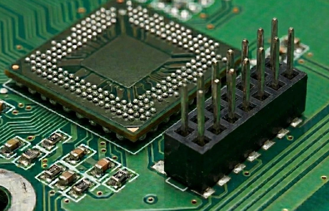
Application Scenarios: Covering all fields from home appliances to aerospace
Wave soldering is widely used in scenarios requiring through-hole mounting:
• Consumer Electronics: Soldering power modules for routers and set-top boxes.
• Automotive Electronics: Soldering connectors for ECUs (Engine Control Units), requiring compliance with extreme environmental conditions from -40℃ to 150℃.
• Industrial Control: Soldering relay modules for PLCs (Programmable Logic Controllers), emphasizing long-term stability.
• Aerospace: Soldering satellite power boards, requiring rigorous testing including vibration and thermal cycling.
Future Trends: The Dual Evolution of Intelligent and Green Manufacturing
As electronics manufacturing evolves towards higher precision and reliability, wave soldering technology is incorporating more innovative elements:
• Selective Wave Soldering: Precise control of flux and solder through nozzles solves the challenges of soldering tiny components.
• Digital Monitoring: Real-time monitoring of wave height and temperature profiles using IoT sensors enables closed-loop process control.
• Lead-Free Depth: Development of low-melting-point lead-free alloys (such as Sn-Bi-Ag) reduces energy consumption and thermal shock risks.
From its initial application in electron tube soldering in the 1950s to its current role supporting cutting-edge fields such as 5G base stations and new energy vehicles, wave soldering has consistently driven advancements in electronics manufacturing technology with its “dynamic wave.” It is not only a paradigm of industrial automation but also humanity’s ultimate pursuit of the “art of connection”—witnessing the perfect fusion of technology and craftsmanship in the flow of liquid metal.