In today’s booming modern electronics manufacturing industry, surface mount technology (SMT) has become a core process in PCB assembly, supporting the massive system of large-scale electronic product production with its high efficiency and precision. However, a shocking statistic serves as a stark warning: according to the Global Surface Mount Technology Association, a staggering 74% of defects in the entire SMT process originate from the solder paste printing stage. This stage, like Achilles’ ankle in Greek mythology, may seem insignificant, but it has become the most vulnerable and problematic point in the entire SMT process.
With the continuous upgrading and replacement of electronic products, high density and miniaturization have become significant trends in their development. Traditional 2D inspection technology is proving inadequate in the face of this new trend and cannot meet today’s stringent inspection requirements. Against this backdrop, this article will delve into the technical shortcomings of 2D SPI, elaborate on the revolutionary breakthroughs brought by 3D SPI, and understand the key technologies for high-precision solder paste inspection.
The Fatal Flaw of 2D SPI: Limitations of Planar Inspection
Basic Principles of 2D Inspection
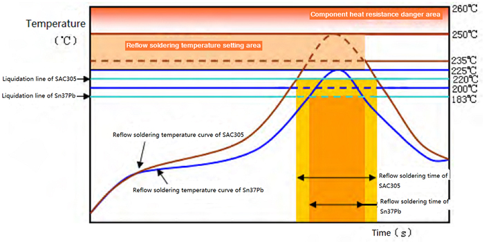
Traditional 2D SPI (Solder Paste Inspection) relies primarily on top lighting and camera imaging technology. Like a “planar detective,” it can only observe the solder paste from above, primarily checking for size, positional misalignment, missing areas, and obvious bridging. However, this method is like looking at the world through a thin veil, only seeing partial planar information and being powerless to address three-dimensional issues such as height and volume.
The Technological Revolution of 3D SPI: A Leap from Planar to Three-Dimensional
Core Parameters of 3D Inspection
3D SPI technology is like an expert in three-dimensional inspection, capable of comprehensive and accurate inspection of solder paste from multiple dimensions. Its core parameters are astonishing:
Height: Possesses ultra-high resolution, enabling precise measurement of minute height changes in the solder paste, like measuring the height of an object with an extremely fine ruler.
Volume: High measurement accuracy allows for precise calculation of solder paste volume, ensuring the exact amount of solder paste used.
3D Shape: Capable of completely reconstructing the 3D contour of the solder paste, providing a clear view of its shape and distribution, like taking a comprehensive “photograph” of the solder paste.
Coplanarity: Accurately measures the height difference between multiple solder joints, ensuring the flatness of the soldering surface and avoiding soldering problems caused by inconsistent heights.
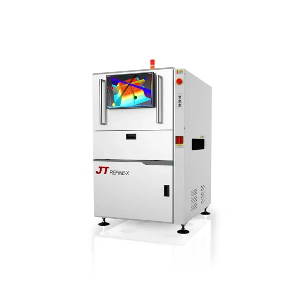
JT 3D SPI – An Essential Option for High-Quality SMT Production
As electronic products continue to evolve towards miniaturization and high density, the requirements for SMT quality control are becoming increasingly stringent. 2D SPI, due to its technological limitations, can no longer meet today’s production demands. 3D SPI, with its leap from planar to three-dimensional, offers advantages such as three-dimensional full-parameter inspection, intelligent early warning systems, and process optimization capabilities. It can completely eliminate the blind spots of 2D inspection, achieve preventative quality control, and continuously improve process efficiency.
JT 3D SPI, as an outstanding representative of 3D SPI technology, helps customers achieve significant results in reducing defect rates, rework costs, and increasing first-pass yields through its five core technological advantages. In the future of electronic manufacturing, 3D SPI will undoubtedly become an essential option for high-quality SMT production, providing strong technical support for the development of the electronics industry.