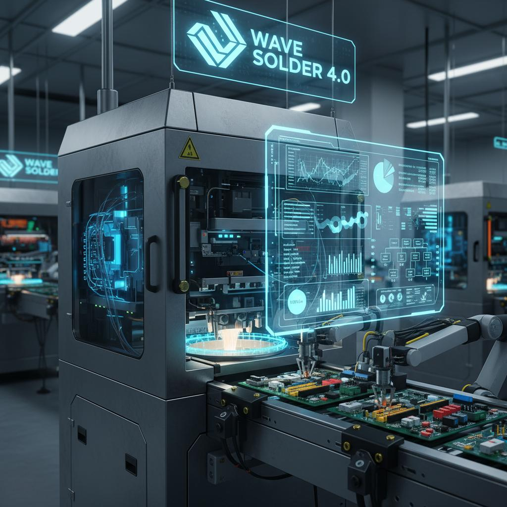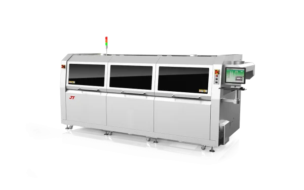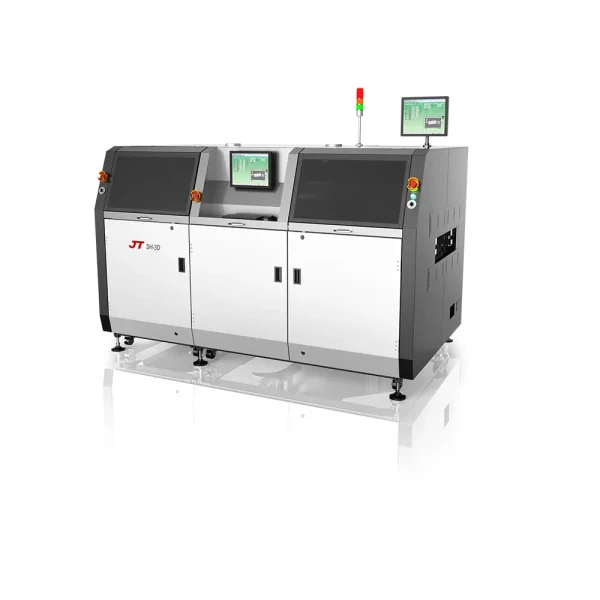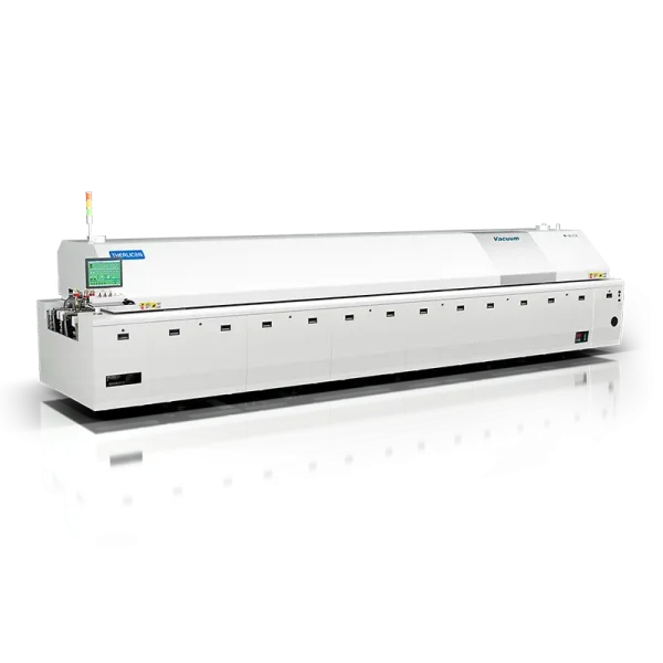

Wave soldering oven is a core automated equipment in printed circuit board (PCB) assembly manufacturing, specially used for batch soldering of through-hole components and partial surface-mounted devices on PCBs. It realizes reliable mechanical and electrical connections between component pins and PCB pads through the continuous flowing molten solder wave, and has become an indispensable process equipment in the electronics manufacturing industry due to its high efficiency and stable soldering quality.

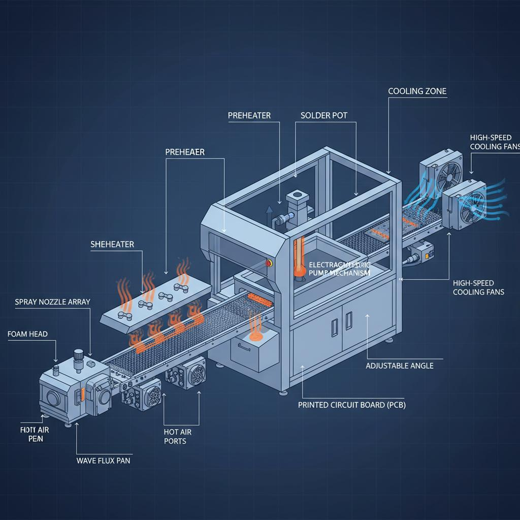
The working principle of wave soldering oven is based on a continuous and controllable four-stage process flow, namely flux spraying, preheating, wave soldering and cooling, with the molten solder wave generation and solder bonding mechanism as its core.
Before formal soldering, the flux spraying stage starts first. The flux sprayer inside the oven evenly coats a layer of soldering flux on the bottom surface of the PCB. The flux plays two key roles: it removes oxide films on the surfaces of PCB copper pads and component pins, and prevents re-oxidation during high-temperature soldering, laying a foundation for effective wetting of molten solder.
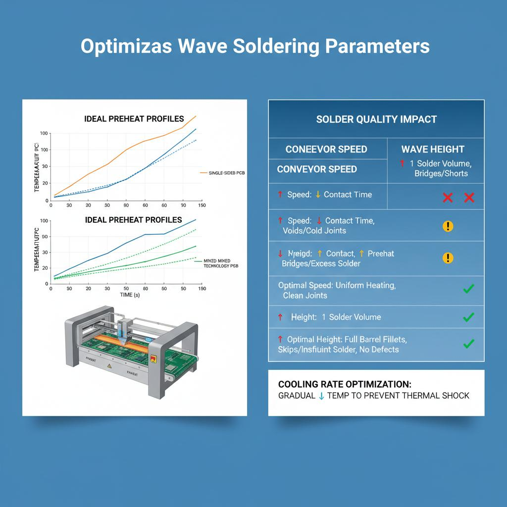
Subsequently, the PCB enters the preheating zone of the oven. The preheating system adopts infrared or hot air heating, raising the temperature of the PCB and components to 100-130°C at a uniform rate. This stage not only activates the chemical activity of the flux to maximize its cleaning effect, but also reduces the temperature difference between the PCB and high-temperature molten solder, avoiding thermal shock that may cause PCB deformation or component damage. At the same time, preheating evaporates trace moisture on the PCB surface, preventing solder spattering during subsequent soldering.
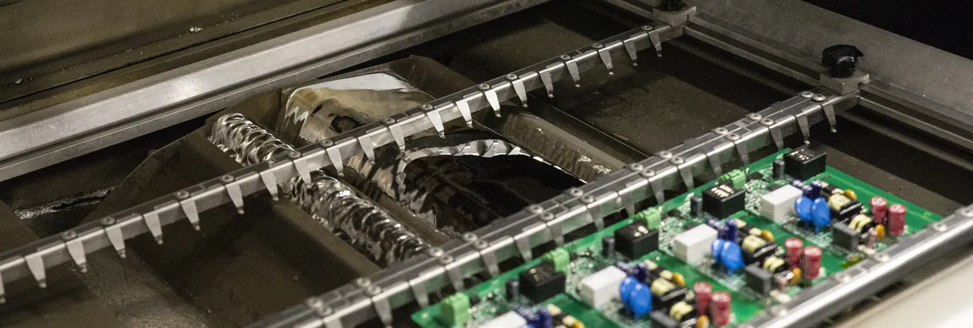
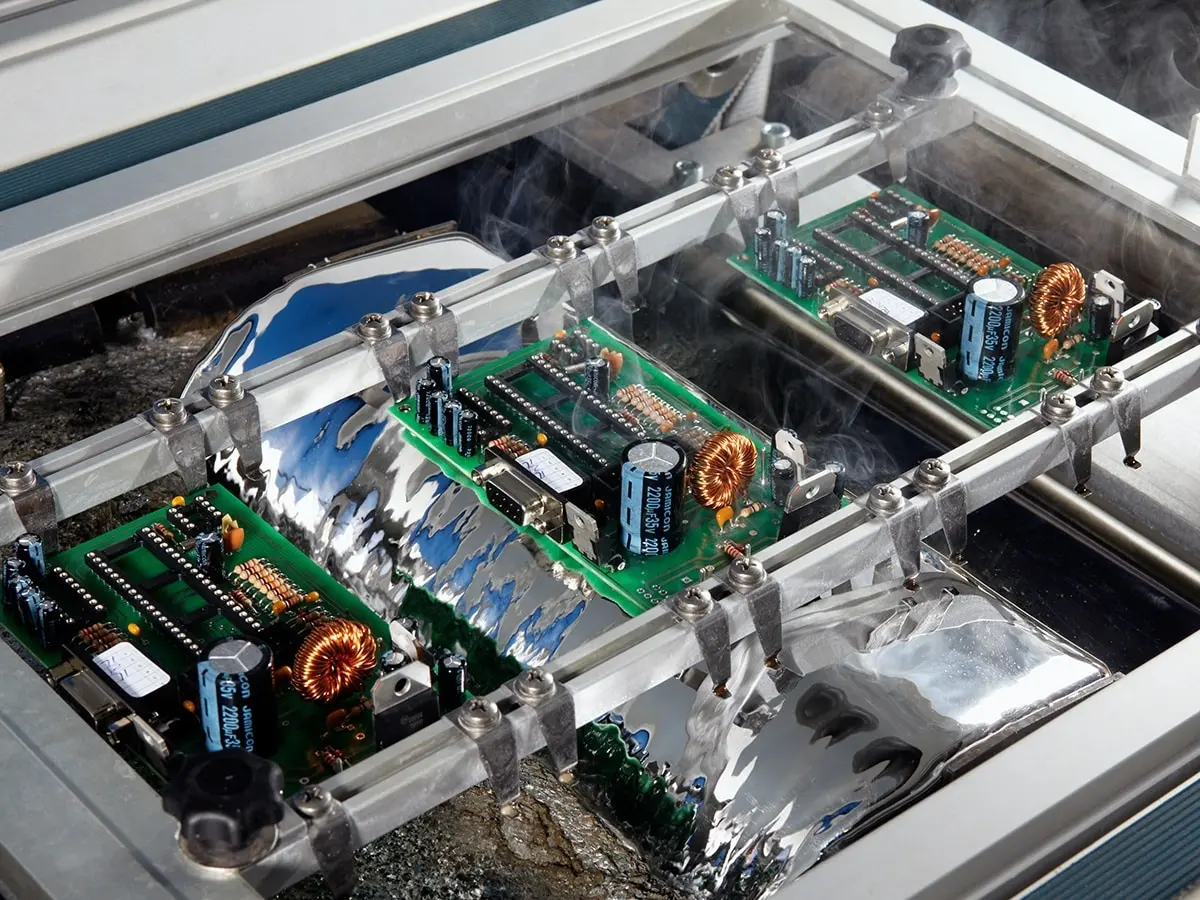
The core of the wave soldering oven lies in the soldering zone. Inside the equipment, a solder pot holds tin-lead or lead-free solder alloy, which is heated to 250-260°C to form uniform molten solder. An electromagnetic or mechanical pump inside the solder pot pressurizes the molten solder, spraying it out from a specific nozzle to form a stable, continuously flowing dynamic solder wave. The PCB is conveyed by a transmission system at a fixed angle (5-7°) and speed (1-2 meters per minute), passing over the solder wave.
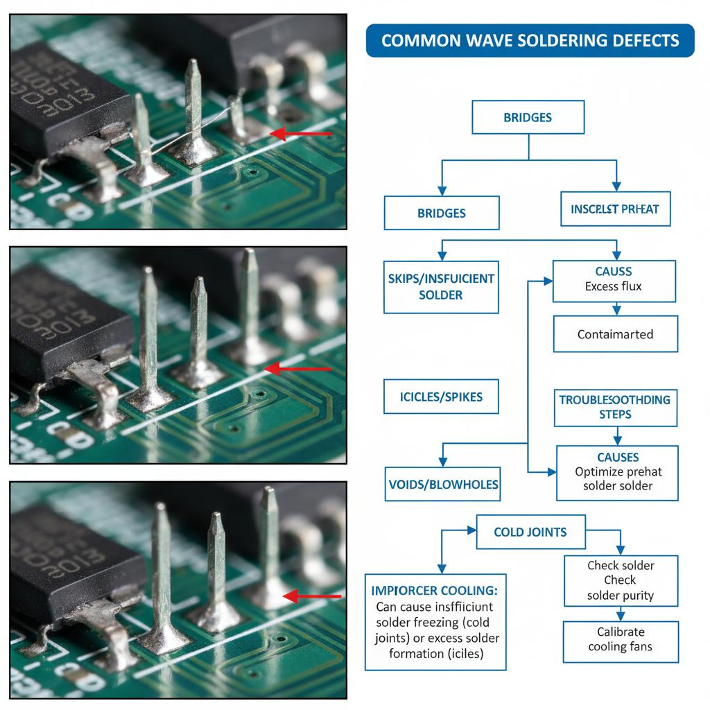
During this process, the molten solder completes the soldering reaction relying on surface tension and capillary action. The solder fully contacts the clean pad and component pins, quickly wets the metal surface, and fills the gaps of through-holes under capillary force. At high temperatures, the molten solder forms a thin intermetallic compound layer with copper on the PCB pads, realizing firm metallurgical bonding. Modern wave soldering ovens mostly adopt a dual-wave system: the first turbulent wave breaks air bubbles and ensures solder penetration, while the second smooth wave trims excess solder and forms neat solder joints, effectively avoiding defects such as cold solder joints and missing soldering.
Finally, the PCB enters the cooling zone. The forced air cooling system rapidly cools the soldered PCB at a controlled rate, making the molten solder solidify quickly to form stable solder joints. Controllable cooling can reduce thermal stress inside the PCB, prevent warpage of the circuit board and damage to components, and ensure the dimensional stability and mechanical strength of the finished product.
In summary, the wave soldering oven realizes efficient and stable PCB soldering through precise coordination of temperature control, power control of solder wave and transmission speed control. Its working principle integrates chemical cleaning, heat conduction, fluid dynamics and metallurgical bonding, which not only meets the mass production needs of electronic products, but also guarantees the consistency and reliability of solder joints, making it widely used in consumer electronics, industrial control, automotive electronics and other manufacturing fields.